The development of NAND flash technology has been steadily moving forward based on a multitude of inputs from the industry. Collaboration between host device solution providers and storage device manufacturers stimulated the establishment of standardized interfaces that were followed and jointly built upon until today’s eco-system.
The two most prominent publicly available interface standards are the Open NAND Flash Interface (ONFI) and Toggle standards, each developed and continually expanded by its respective prestigious workgroup. While contrasts and comparisons can be drawn between the two standards, a well-recognized “common ground” is the JESD230 standard, published by the Joint Electron Device Engineering Council (JEDEC), which can be utilized as a reference that developers extract from the standard sets.
The unique development of each set of standards is apparent by the differences in commanding, addressing, timing, formatting, and physical configurations due to their shaping under distinct scopes and knowledge of groups of leaders in the flash and storage industry. Nevertheless, both standards channel cohesiveness in their striving for compatibility and interoperability among different technologies.

The legacy interface
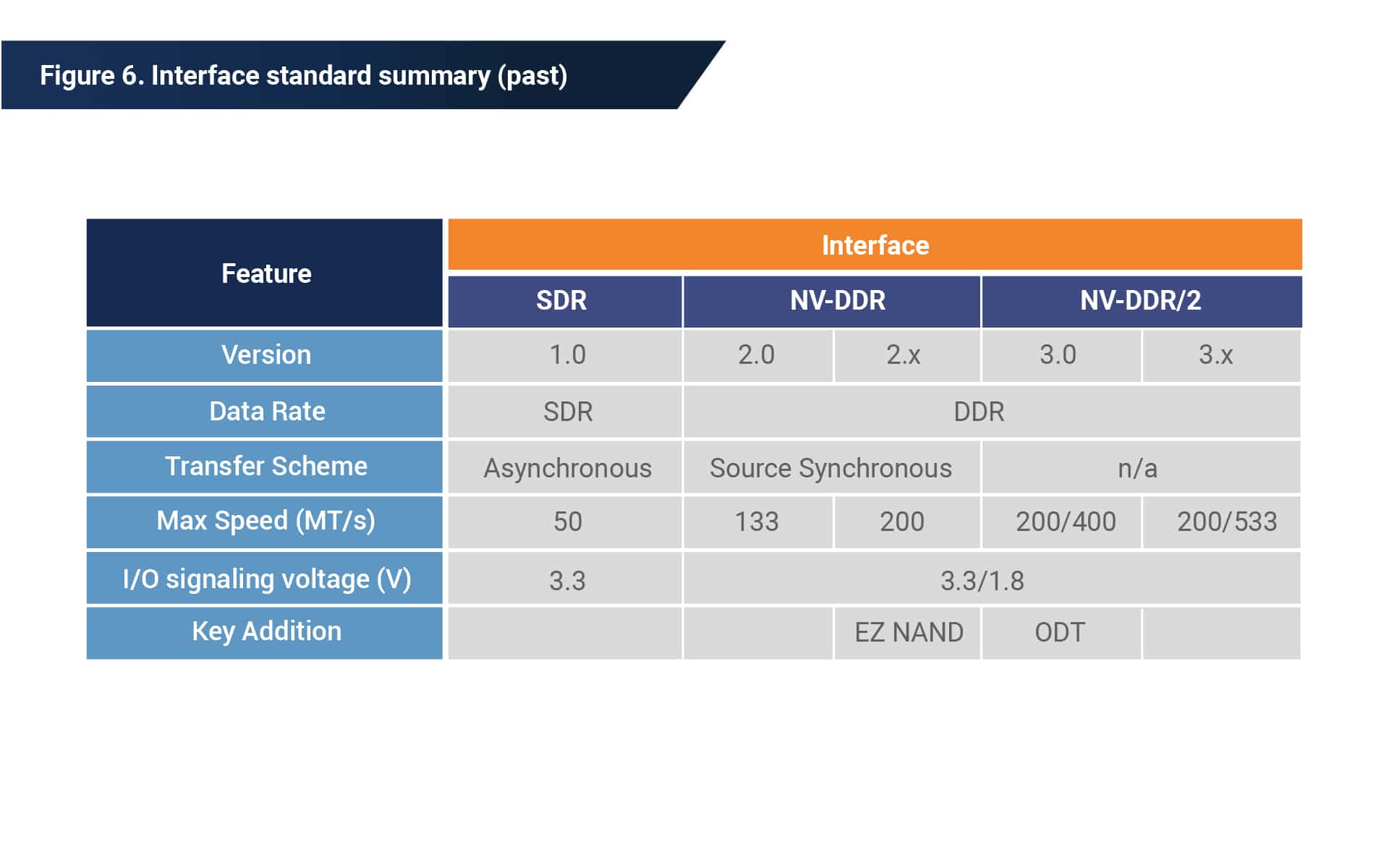
Delving into the pool of flash interface knowledge, you can immediately identify the comparison between synchronous and asynchronous data transfer schemes. The first NAND Flash Device Interface, known as Legacy, was configured to utilize the asynchronous transfer scheme related to the timing criteria for data transfers. For enhanced signal integrity and accuracy, a synchronous scheme is used to control the signals that need to be synchronized with a continuous clock signal. The asynchronous scheme allows the triggering of transfer tasks to be wholly dependent on “Write-Enable (WE)” and “Read-Enable (RE)” control signals without the need for a clock.
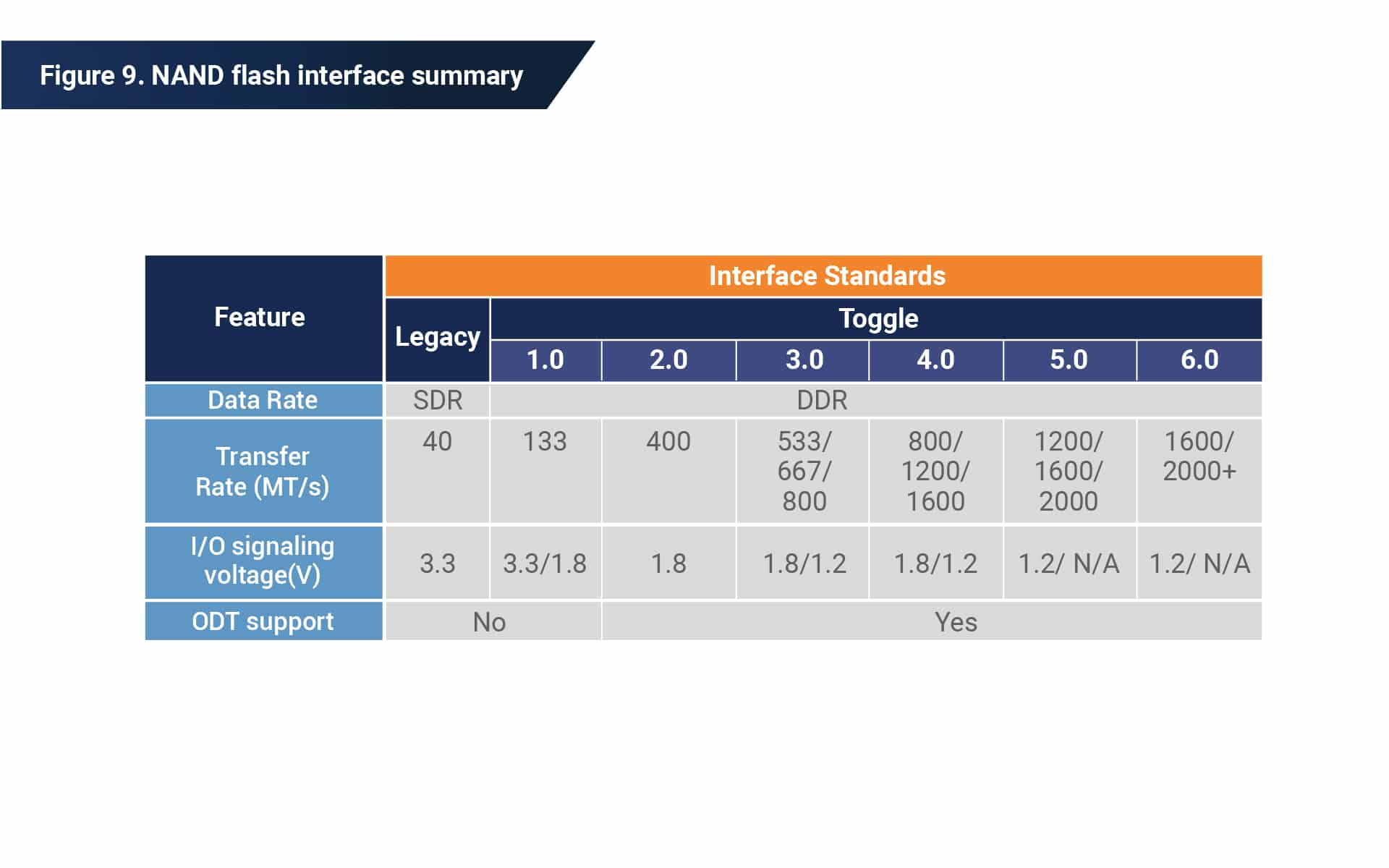
In addition, Legacy supports data transferring on Single Data Rate (SDR), processing data transfer only upon one edge of control signals. Specifically, the interface enforces formulated signal alignments only on the rising edges of write signals and the falling edge of read signals as data is “moved” in and out of devices.
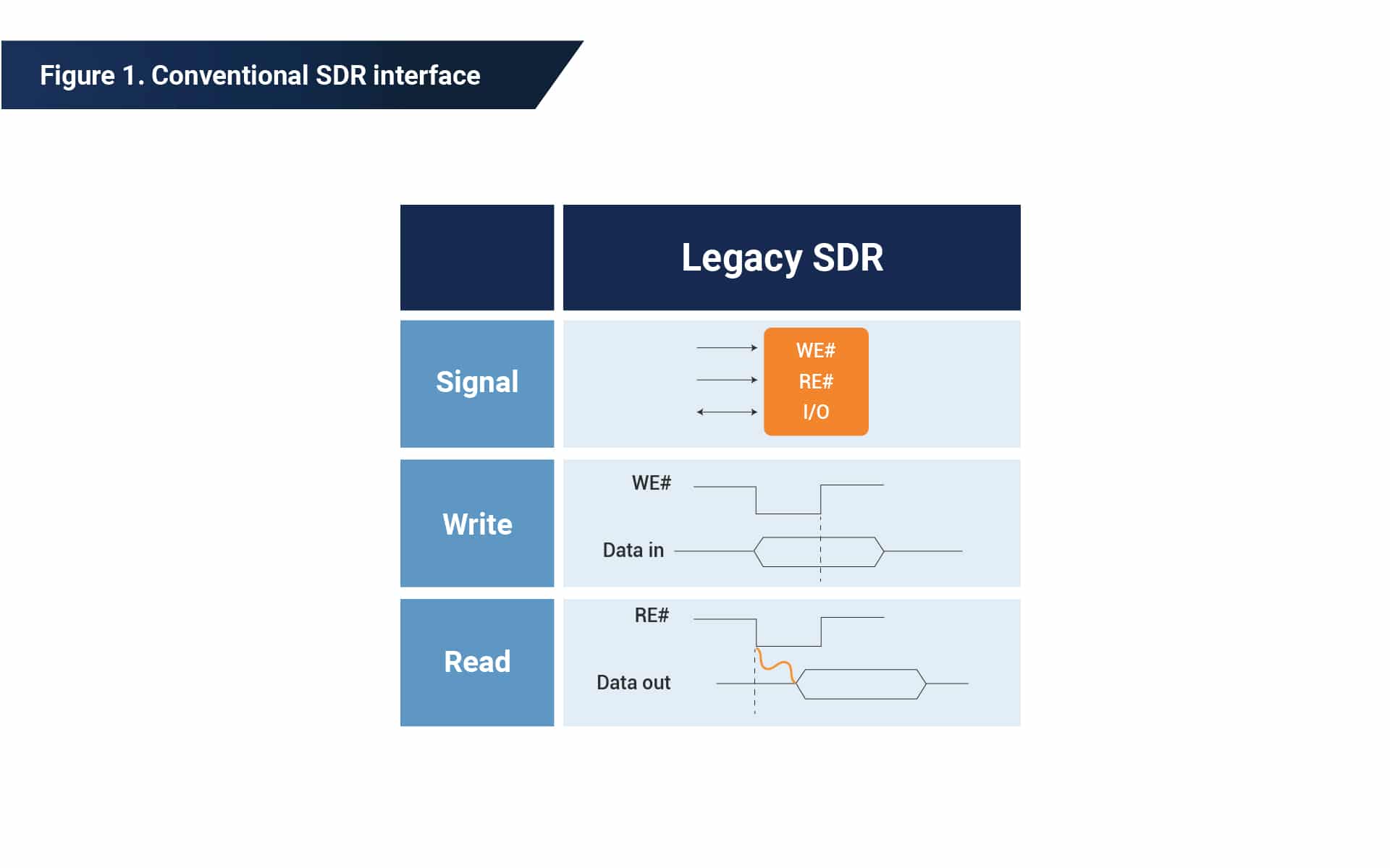
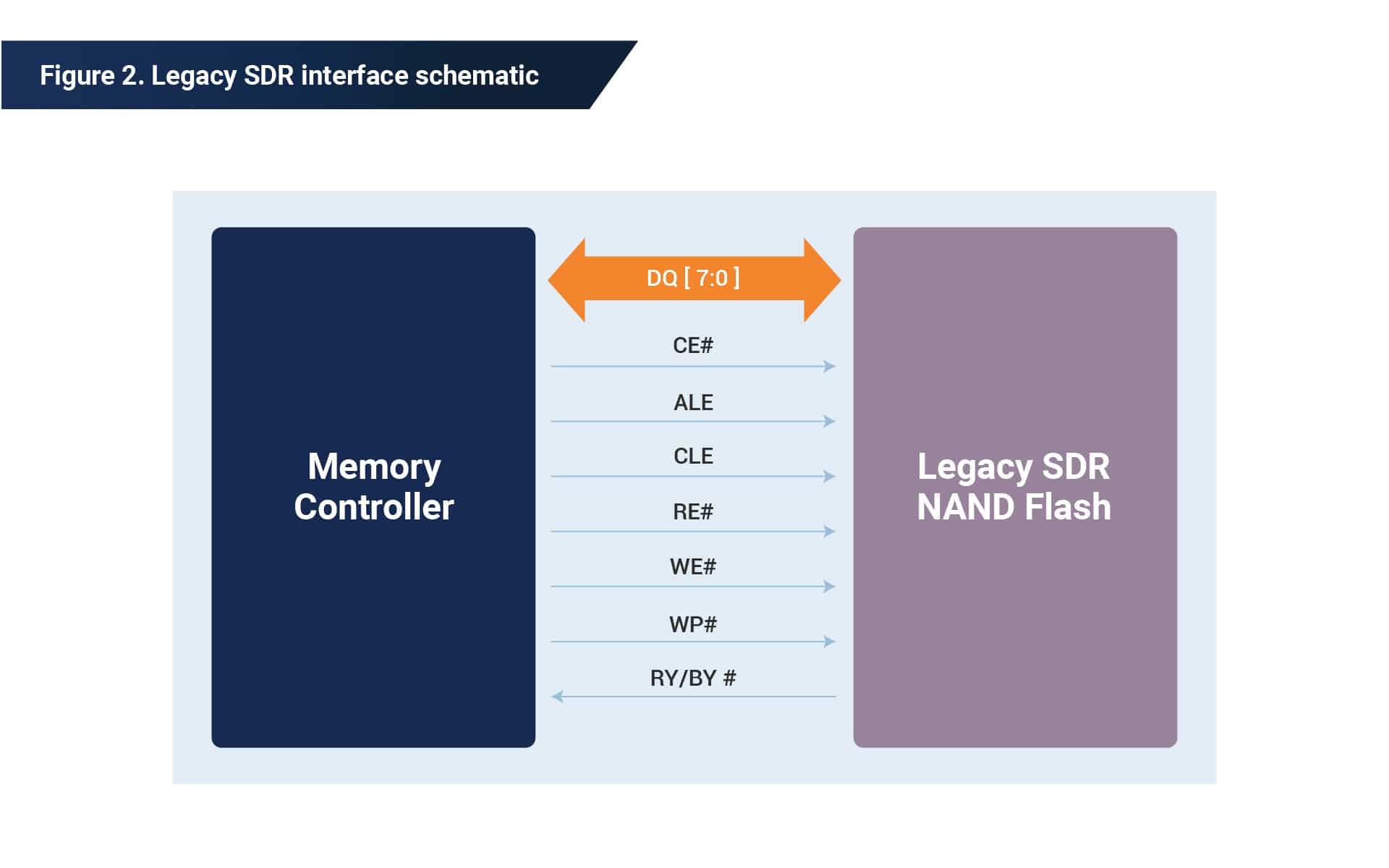
With seven control signal pins in addition to an 8-bit(b) bidirectional data bus for I/O signaling (DQ), the 15-pin interface accomplishes the delivery of a byte(B) within a transfer time of 25 nanoseconds(ns). Building on this attribute, the maximum bandwidth can be calculated as 40MB/s or 40Mb/s per data pin. (1B/25ns = 0.04×10⁹ B/s = 40 MB/s, 1B = 8b)
The ONFI interface
In 2006, a large group of tech companies formed the Open NAND Flash Interface (ONFI) Working Group, including SK Hynix, Intel, Micron, SanDisk, Phison, Sony, and others. Later that year, the first version of the ONFI standard was drafted and released, targeted to provide a unified standard in response to the disorganized nature of the flash market (stemming from the inconsistent criteria for flash interfaces between storage products, flash vendors, and downstream product manufacturers).
The multi-faceted ONFI standard illustrated crucial aspects of a proper interface the market desperately needed, including but not limited to function characterizations, feature/command set regulating, signal description/timing conditions, behavioral flows, and register-level/physical specifications. Today, the ONFI Workgroup continues to release updates to expand from the set of standards, with the most recent draft being ONFI 5.0 as of 2021.
ONFI 1.0
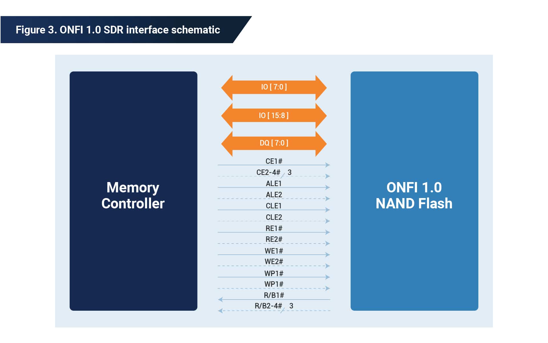
The primary purpose of the first release was to supply an expedited interface standardization extended from Legacy. While hovering with the asynchronous SDR transfer scheme, version 1.0 described an electrical interface similar to the conventional Legacy but with optional support of cutting-edge technologies such as a 16-bit data bus with control signals up-scaling. The bandwidth of 50MB/s marked a 20% improvement over the previous 40MB/s performance of Legacy.
ONFI 2.0
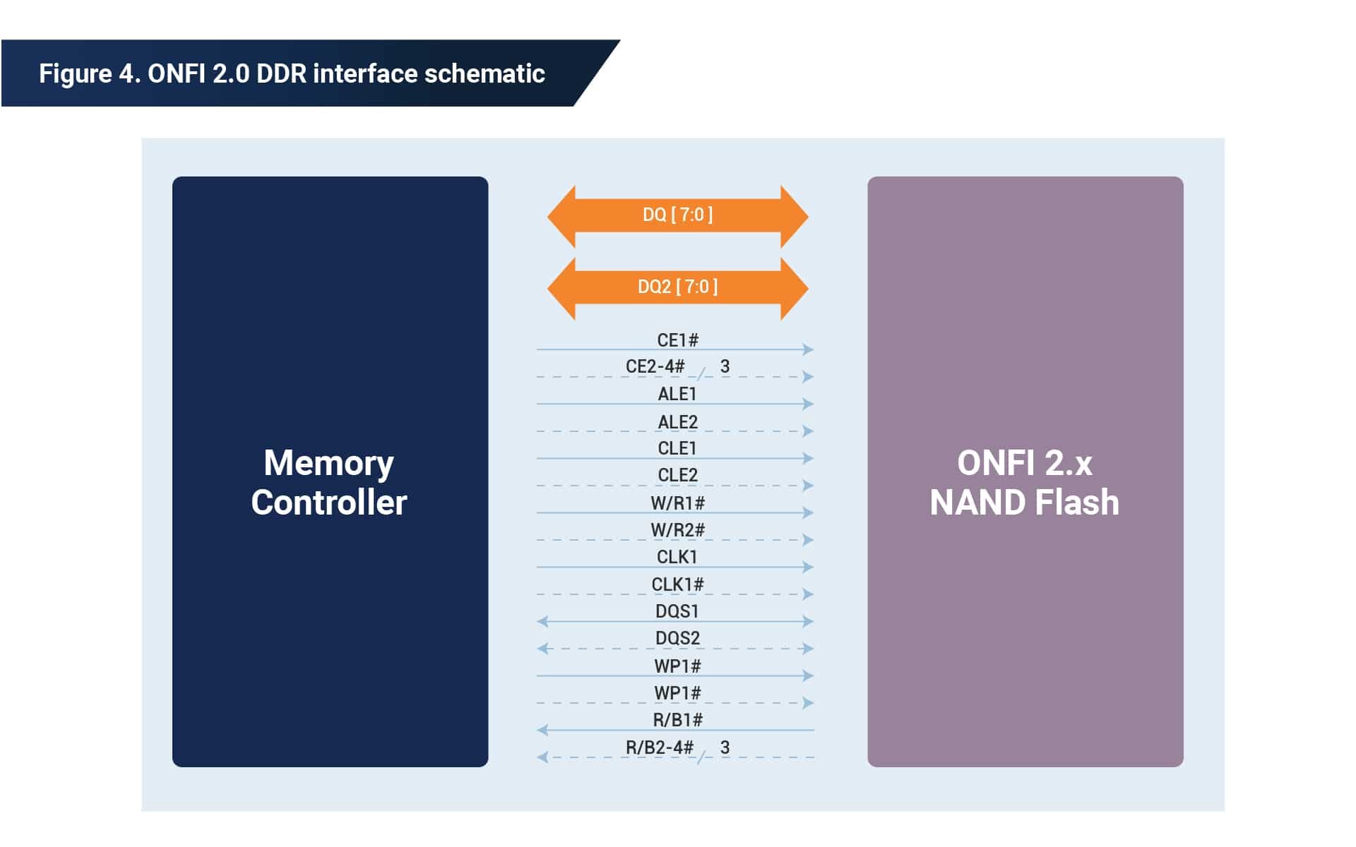
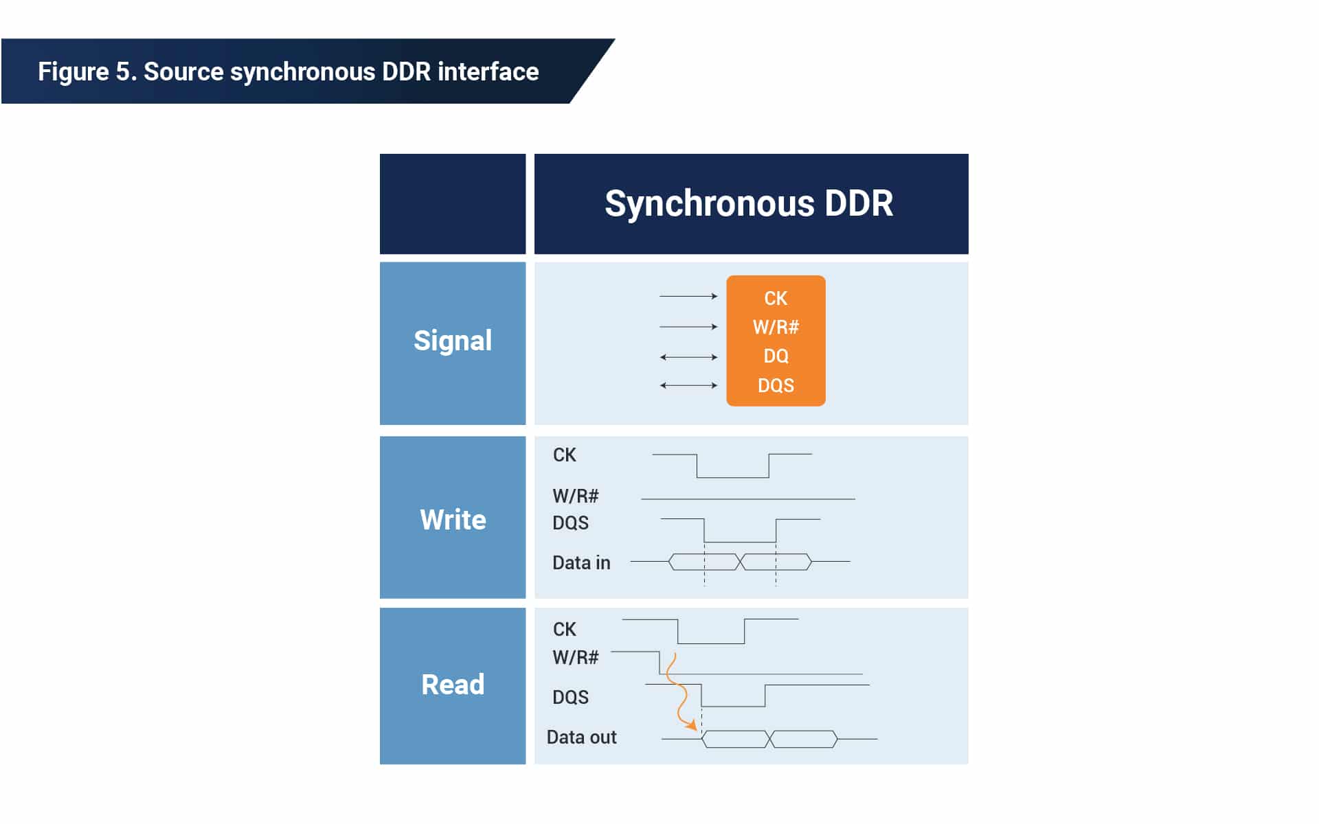
ONFI 2.0 was released in February 2008. The most significant change was the adoption of the Double Data Rate (DDR) transfer scheme that enabled a substantial increase of device maximum throughput by allowing data transfers upon both edges of control signals. Moreover, the ONFI standard rectified the DDR Flash Interface within this specification as the NV-DDR (Non-Volatile DDR) interface, allowing it to be differentiated from the volatile memory DDR interface utilized by Random Access Memory (RAM).
Although NV-DDR retained the asynchronous working scheme for backward compatibility with the preceding SDR revision, adjustments were made to support the source-synchronous scheme. Specifically, the former WE control signal became the clock signal (CLK), while the RE control signal became a direction signal to select between read and write operations. In addition, data was now transferred on both rising and falling edges of the newly added data strobe signal (DQS) to achieve the doubled rate of transfer up to 133MT/s. The increased throughput promptly addressed the trend for data transfers of larger sizes and random performance improvement.
ONFI 2.1
ONFI 2.1 was ratified in 2009 with expansions on multiple sections of the 2.0 revision. The 2.1 standards enabled maximum transfer rate upgrade to 200MT/s in addition to new features that provided room for operational flexibility.
Multiple sections within the ONFI specification were expanded, beginning with extended parameter pages that report error correction coding (ECC) capabilities. As a key addition in revision 2.1, the extended ECC information allowed multiple valid usage methods for a NAND device under specified pairings of ECC parameters with other device parameters, such as the number of valid blocks and the number of program/erase cycles supported.
Moving on to memory organization, the introduction of interleaved addressing and logical unit number (LUN) opened up engineering opportunities in addition to reduced package pins, specifically the chip-enable pins, decreasing the redundancy of complex hardware design.
The “Small Data Move” and the “Change Row Address” were introduced as device control commands. The “Small Data Move” command addressed the ECC limitations for low-end consumer applications with downsized data chunks in device control commands. The “Change Row Address” command was aimed to reduce workload overhead by increasing device operational flexibility.
ONFI 2.2
Building on the changes from the preceding revision, ONFI 2.2 was released at the end of 2009 with additional guidelines on memory organization. Restrictions on the previously introduced interleaved addressing were stated, and reset commands for individual LUNs were added. The revision also defined a current measurement methodology within the specification’s appendix.
ONFI 2.3
ONFI 2.3 was released at the Flash Memory Summit (FMS) in August 2010 with a focus on the EZ-NAND (ECC Zero NAND) protocol. The protocol advised shifting ECC management units from the storage controller side to the flash side, thus relieving the pressure from the burdened control unit.
ONFI 3.x
ONFI 3.0 was announced in March 2011 with an ambitious leap in supported transfer rates of up to 400MT/s, suitable for the 8K page data alignment size increase trend favored at the time. The throughput upgrade also came with reduced signal voltage to 1.8-volt as a step toward power consumption optimization.
Many other new features were introduced to elevate the ceiling for flash innovation. On-Die-Termination (ODT) led the way as the more impactful addition in this spec revision as a design that improved signal integrity of memory channels by allowing the controller to turn on and off the termination resistance for independent or all devices within a package. Multi-die package capabilities like ODT were addressed in detail within this revision to govern delicate die-level operations and behaviors.
Other features included volume addressing enhancements and a decreased number of required chip-enable pins, which improved circuit routing efficiency. Yet as revision 3.2 was released, a transfer rate upgrade again captured the spotlight as the 533MT/s throughput became available under the NV-DDR2 interface, which at the time legitimized flash upgrades within devices of the same generation.
ONFI 4.0
The ONFI 4.0 specification arrived in 2012 with transfer rate upgrades to 667 MT/s by the formerly-known NV-DDR2 and 800MT/s by the newly-introduced NV-DDR3. A technique referred to as ZQ calibration was introduced as an ODT facilitation tool to calibrate the termination resistance. This specification limited the compromising of signal integrity in cases of voltage or temperature changes. Moreover, these enhancements allowed the I/O power (VCCQ) requirement to reach down to 1.2-volt for improved power consumption.
ONFI 4.x
ONFI specifications extended from version 4.0 harbored several changes, including power configuration flexibility, subsidizing feature parameter definition, and additional physical pin assignment options.
Starting with ONFI 4.1, options for core control voltage(VCC) were opened up as 2.5-volt, and a range of configurations from 2.35-volt to 3.6-volt was added to the original 3.3/1.8/1.2 settings.
Duty Cycle Correction (DCC) and DQ Read/Write Trainings were added on top of ZQ calibration as features to facilitate NAND device adjustments during the initialization process. This change specifically targeted devices operating over 800MT/s with heavy workloads. DCC trainings were targeted to compensate for potential duty cycle mismatches of the “Read Enable Complement” signal (a complementary signal to the “Read Enable” signal). The
DQ trainings served as an attempt to align the DQS and DQ signals with the host-side system.
With the 4.2 revision, modifications on the details of DCC training specifications were made, while other changes occurred in the physical pin assignment options. Specifically, a 252-ball ball-grid-array (BGA) assignment joined the former BGA-272 and BGA-316 assignments as a new option for the physical interface.
ONFI 5.0
The release of ONFI 5.0 came in early 2021. Three more pin assignment options were revealed in the freshly released standard specification, along with instructions on changes required for proper adoption. But more important was the NV-LPDDR4 interface, emphasizing lowering overall power consumption while upscaling the transfer rate of each interface, namely 800 MT/s by NV-DDR2 and up to 2400MT/s by NV-DDR3 and NV-LPDDR4. With allowance from the increased transfer rate, devices supporting NV-LPDDR4 can utilize the Data Bus Inversion (DBI) function to limit power consumption by controlling the signal directions and thus the amount of current flow.
On the other hand, the arrival of NV-LPDDR4 triggered another push for feature modification for ODT. Additional features like ODT Disable/Enable and Channel ODT addressed potential impacts ODT sustained from the new NV-LPDDR4 interface.
On the enabling of NV-LPDDR4, the internal reference voltage between NAND devices and controllers could be left at an untrained state, but the small signal swings caused by ODT could lead to failure in command sequences. Therefore, properly timed ODT disabling/enabling can significantly influence operations under the new interface.
Apart from this switch-like feature, the channel ODT setting grants control to the on-NAND output pull-up resistor strength and thus the signal termination resistance. In other words, the setting essentially allows the host-side to decide the optimal ODT strength within each channel during data output operations. At the same time, the NAND devices adjust accordingly based on vendor-specific setting values.

The toggle interface
In the year immediately following the release of ONFI 1.0, Samsung Semiconductors and Toshiba Memory Corporation (TMC), two of the world-leading NAND flash manufacturers, introduced the Toggle interface standard as an alternative to drive flash device operations beyond Legacy capabilities. Devices utilizing the Toggle interface also operate on a set of expandable, meticulously knitted guidelines in various hardware configurations, signaling patterns, and electrical characteristics. The evolution of the Toggle standard occurred within customer-specific releases of NAND device specifications from Samsung and TMC instead of to the public. This was in contrast to the ONFI standard that was updated based on unified public releases from its workgroup.
Toggle 1.0
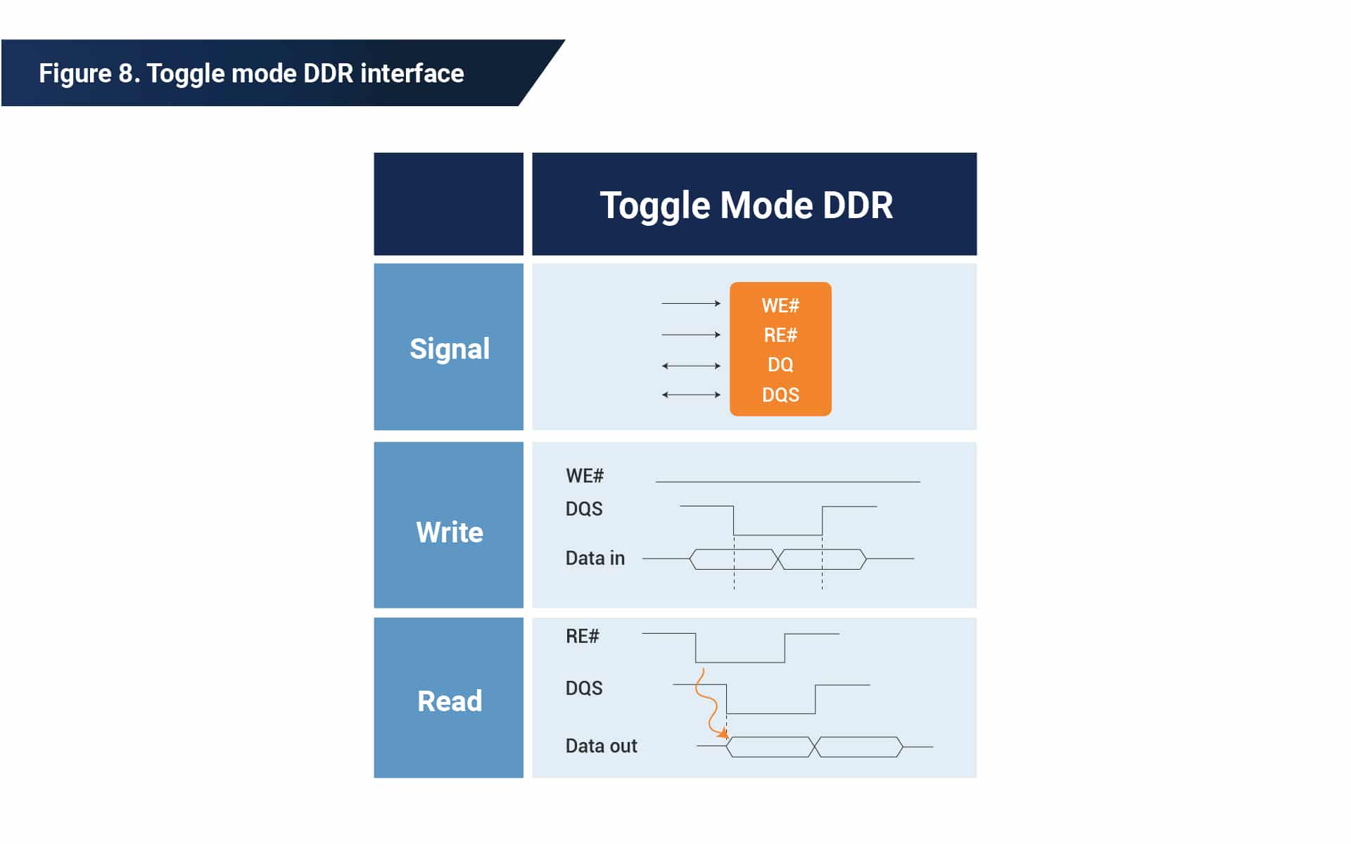
From the first look, the first generation Toggle DDR interface had a hand of general characteristics in common with the ONFI 2.0 revision. Toggle 1.0 allowed data transfer rates of up to 133MT/s using bidirectional DQS strobe signals, with each rising and falling edge being associated with one data transfer. However, the difference between ONFI and Toggle is that the Toggle data transfer is operated without a clock signal, making it asynchronous with power consumption at the occurrence of read and write operations only. ONFI also adopted such implementation with its edge in power efficiency and design simplicity in revision 3.0.
Toggle 2.0 / 3.0 / 4.0
Devices supported by Toggle 2.0 allowed throughput up to 400 MT/s, making them comparable to those operating under ONFI 3.0. Yet only a portion of the Toggle 2.0 devices supported the ODT feature depending on the release timing.
While Toggle 3.0 devices came along in 2015 with supported transfer rate options of 533MT/s and 667MT/s and full support of ODT and ZQ calibration features, the mainstream Toggle standard revision is the Toggle 4.0 standard. At its earliest release, the Toggle 4.0 interface enabled transfer rates up to 800MT/s and 1200MT/s while supporting the necessary features matching ONFI but with varying illustrations depending on products.
Of course, the interface standards were designed to target the most recent NAND flash technology, namely, the BiCS-series for Kioxia (formerly TMC) and Western Digital, and the V-NAND series for Korean suppliers such as Samsung and SK Hynix. As a matter of fact, with new flash designs and technology rolling out, the flash vendors have been able to tune up the transfer rates by calibrating flash behaviors through repeated trial-and-errors within the same generation interface. Phison has been collaborating with its flash vendor partners to see the transfer rate breakthrough above 2000MT/s, along with various design improvements that have come at the perfect timing as system front-end performance faces the challenges of next-generation interconnects.
Toggle 5.0 / 6.0
The future is bright as developers assiduously pile on the building blocks in the book of standards for flash interfaces. As the 3D flash technology has officially entered the 100-plus-layered stacking era, the industry is looking at an imminent transition to even faster and more cutting-edge interface exchanges speed. Shortly, Toggle 5.0 and 6.0 interfaces are expected to run on transfer rates above 2400 MT/s, translating to above 250 MB/s per die. With flash topology and design change discussions ongoing, the industry anticipates more feature additions and improvements to advance mainstream standards.
The future of NAND flash
In the past 20 years, ONFI and Toggle NAND flash interfaces have flourished and been recognized as the industry standard for developing NAND flash applications. As of 2021, the latest releases from both standards have taken NAND flash performances up to more than ten times the conventional Legacy capabilities while enabling higher module capacity and lowing power consumption. Phison, with more than 1900 worldwide patents and 20 years of flash industry experience, is ready to provide memory controller support to address the needs of any application under either of the two primary interfaces.