Introduction
Over millennia, humanity has developed a well-worn, time-tested formula for making technological advancements. Inventors and designers first concentrate on figuring out the general mechanisms of a new technology before they turn their heads to cost efficiency and performance improvements.
This basic rule of thumb applies to the solid-state storage field as much as to any other discipline or industry. In this article, we’ll explore an important recent development that can help boost the performance of solid-state drive technology: host memory buffer (HMB).
The trade-offs of SSD memory design
In the design of a solid-state drive (SSD), extra flash memory can increase the overall drive capacity while raising performance. Like any other product design, however, engineers must make a trade-off between resources and costs.
For SSD design, there are two ways to improve the performance of each unit beyond its existing capabilities: either by increasing the density of flash memory or by mounting additional flash memory at the cost of extra physical space. Since the printed circuit board (PCB) space is limited no matter the choice of drive form factors, however, this usually comes at the cost of omitting other components on the board.
Many vendors now opt to remove the fast yet expensive DRAM (dynamic random-access memory) from their drive designs to achieve cost reductions. However, as a high-speed volatile memory, DRAM has its own purposes and isn’t easily replaceable. A DRAM-less design also has its own issues to face in terms of performance and signal integrity tuning during data transfers, especially within high-volume random read circumstances.

What is host memory buffer?
So how can designers address the weaknesses of a DRAM-less SSD? The concise answer is Host Memory Buffer (HMB) technology. HMB is a technique that allows SSDs to proactively pursue higher performance by utilizing the memory resources of the host CPU.
NVMe (NVM Express or Non-Volatile Memory Express) is an open standard that defines how to access a computer’s non-volatile memory, such as NAND flash memory and SSDs. The NVMe 1.2 specification was the first to introduce the host memory buffer feature.
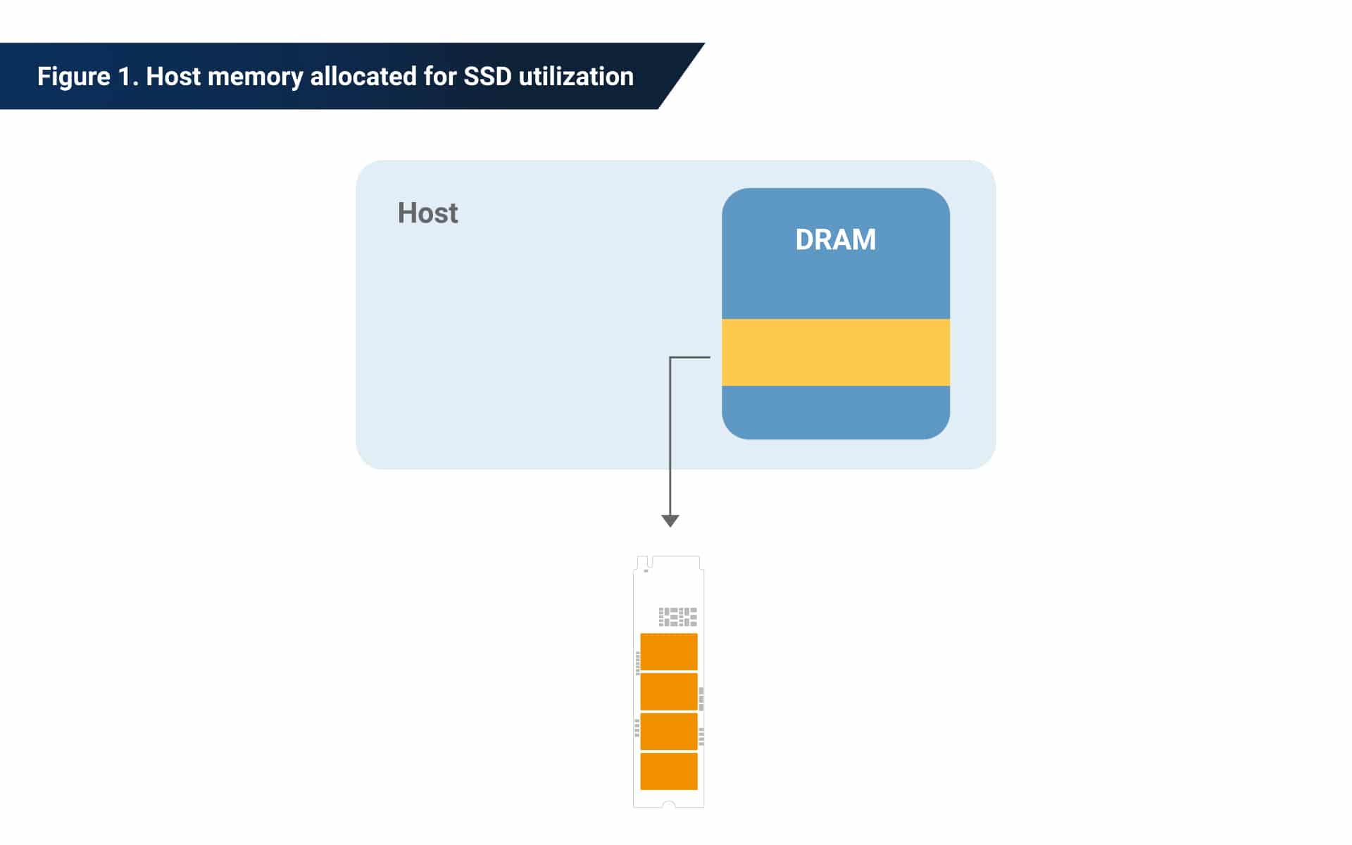
Specifically, NVMe 1.2 outlined how HMB allows host memory to be allocated for the use of SSDs. Any SSD with the proper configuration can communicate with the host to specify the minimum buffer size that it requires. The NVMe 1.2 specification also included conditions and restrictions for various purposes, such as ensuring that data is not lost or corrupted if the drive is accidentally removed.
To use the HMB feature, both the drive and the operating system must support it. Fortunately, Microsoft has allowed HMB support since Windows 10 Creators Update (i.e., version 1703), which was released in 2017.
Why HMB? From with DRAM to without DRAM SSDs
Earlier SSD designs used both non-volatile flash devices and volatile RAM to increase data processing efficiency. Specifically, DRAM devices are used as buffers for two reasons:
-
-
- DRAM devices are volatile and lose track of their data when the power is shut down. This means that RAM is not suitable for long-term data storage.
- RAM devices can be read or written to at a higher speed than flash devices. This attribute allows RAM to serve as a “relay station,” a temporary stop for data from the host, while giving flash storage a reprieve as it continually processes tasks.
-
The most important information that gets cached to or retrieved from a DRAM is the mapping information that turns logical addresses into the physical locations of stored data within the NAND flash array. This information is stored in mapping tables called L2P (logical-to-physical) tables and is updated frequently as SSDs move data in and out of flash storage. During shutdowns, the L2P table is stored in flash memory, since DRAM quickly becomes inoperable without a continuous power supply.
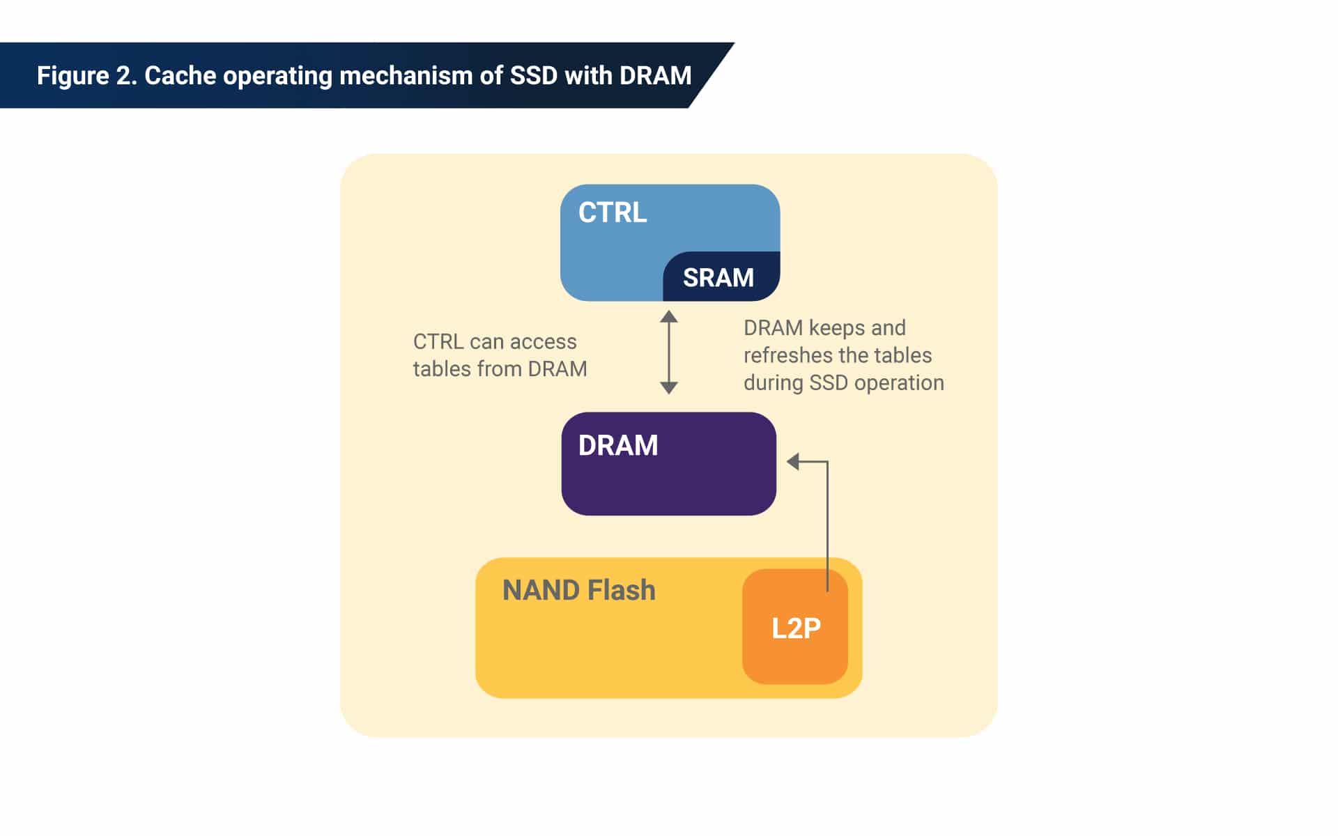
On the other hand, during powered-on scenarios, the L2P table is uploaded to DRAM so that it can be constantly updated by the controller. The larger the DRAM size, the more free space available for the controller to play with. This generally means more flexible data placement and thus better reaction time upon receiving commands. In terms of typical data workloads, operations that call for so-called “random read” sequences benefit the most from ample DRAM space.
However, valuable resources like DRAM come at a high expense compared to flash storage. Controlling for density, current DRAM prices are more than 10 times the average prices of NAND flash memory, and there’s no indication that this will change soon.
Despite the benefits of DRAM, the past decade has seen the introduction of SSDs without mounted DRAM. These “DRAM-less” drives offered advantages such as lower costs and smaller physical dimensions.
But DRAM-less SSDs aren’t exactly a “one-size-fits-all” solution either. The performance of DRAM-less SSDs generally suffers due to innate deficiencies in the caching space reserved for intermediate data and mapping tables.
Although DRAM-less designs also keep L2P tables in NAND memory, they have an important difference from designs with mounted DRAM. As the controller attempts to access these tables from NAND flash memory, the information is loaded into the controller’s internal SRAM (static RAM) as it gets updated and utilized. Afterward, these tables are then again placed in NAND flash memory for storage.
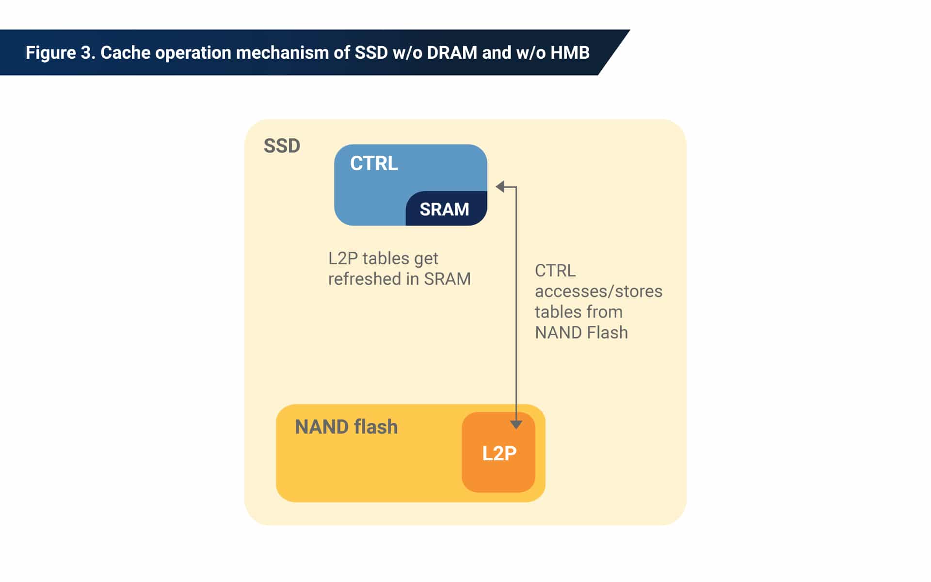
The key distinction here is the use of SRAM as the caching space. However, SRAM is a valuable, high-performance resource with even higher costs than DRAM. What’s more, a typical flash controller usually has only a few megabytes of SRAM. Since larger buffer space typically leads to higher efficiency, these DRAM-less designs may be considered suboptimal from a performance perspective.
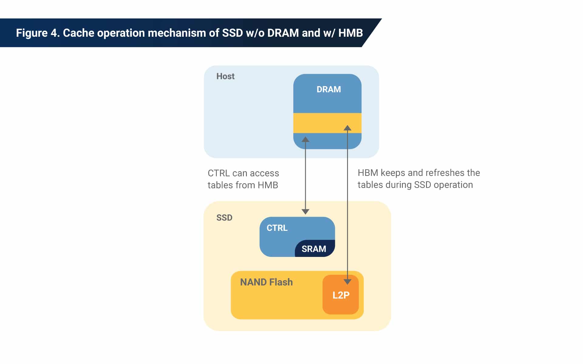
This shortcoming is precisely why the HMB feature was designed. During SSD operations, L2P tables can be loaded directly from NAND flash to HMB. These tables can be refreshed continuously in buffer memory from the host side, almost identically to the conventional DRAM method.
SSDs with HMB enabled generally see significantly less to possibly no degradation in efficiency handling random workloads. In the next section, we’ll explore some concrete real-world testing data on HMB performance.
HMB performance improvements: with vs. without
With HMB enabled, SSDs generally see performance improvements in so-called “random reads.” These operations are when data of a predetermined size (but from unpredictable locations within flash storage) is retrieved per host request via controller-level maneuvers.
However, HMB performance boosts can also vary under different workloads. This is because the host may not always be able to provide the actual amount of internal memory space demanded by the flash controller.
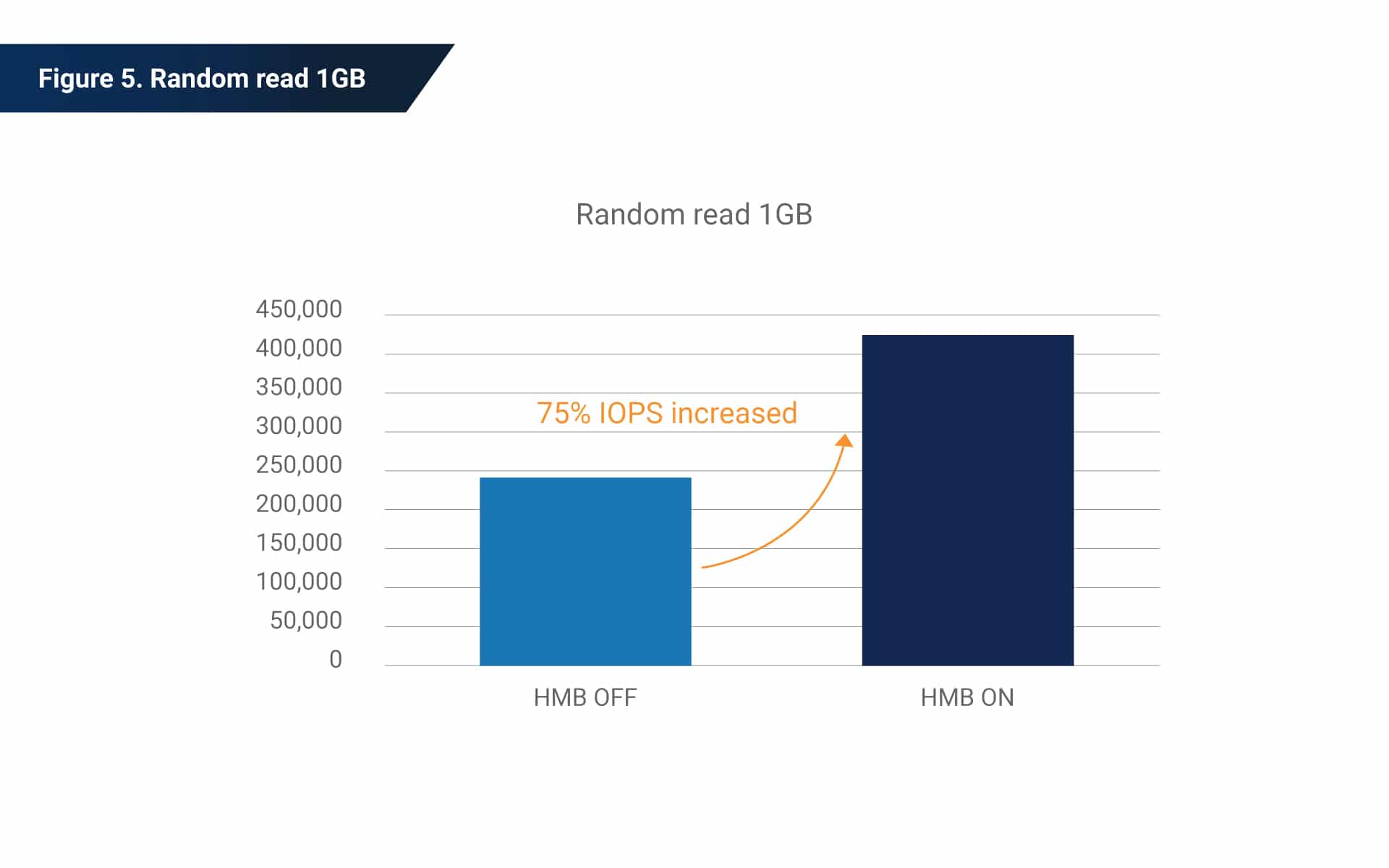
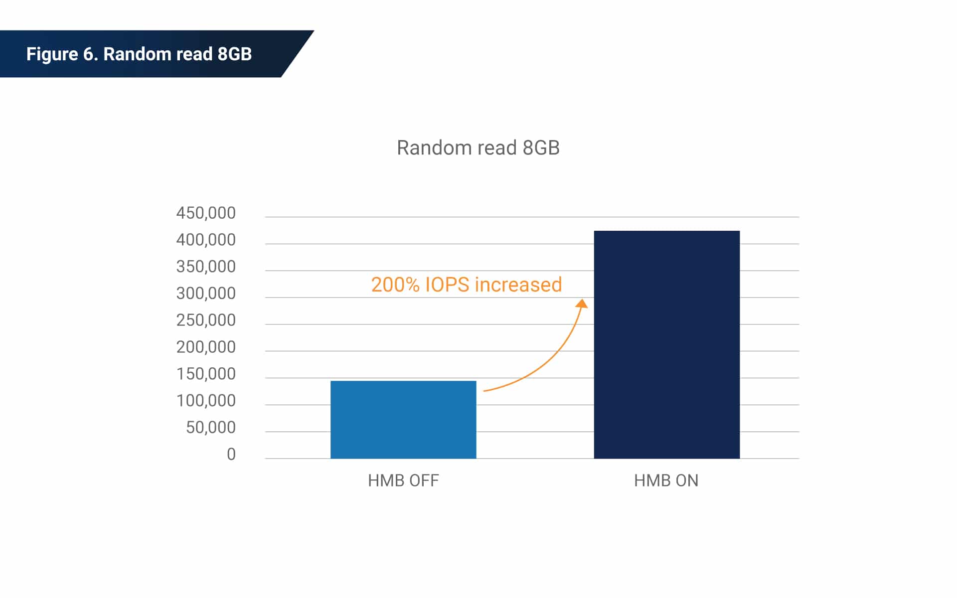
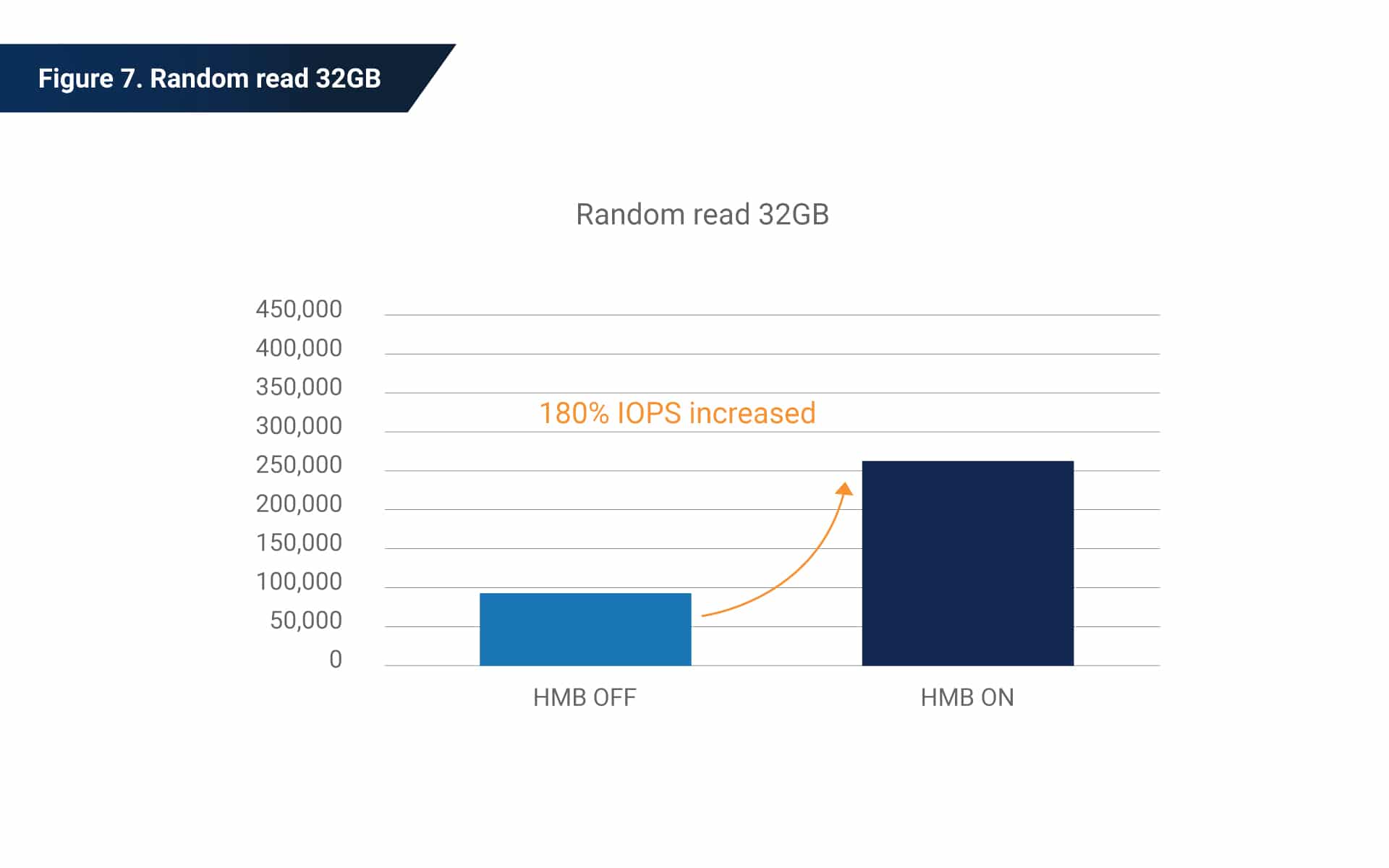
These graphs demonstrate a non-linear performance boost from the use of HMB, scaling up the workload from handling 1 gigabyte worth of data to 32 gigabytes. This is due to the DRAM capacity limitation of HMB.
As we handle the L2P tables and process larger quantities of intermediate data, we reach a threshold where load operations into the provided HMB space begin to grow exponentially. Thus, the increase in IOPS (input/output operations per second) with 32 gigabytes of data is less significant than with just 8 gigabytes of data. This shows that HMB, like any hardware technology, has limits to its performance improvements.
Even with 32 gigabytes, however, we still get more than 100,000 additional IOPS when using HMB. This is easily a significant increase—even painstaking firmware optimization can have a return of only several thousand IOPS.
How Phison uses HMB for the world’s best SSDs
Since they were first released, DRAM-less SSDs have been broadly deployed as part of vendors’ so-called “value line,” offering advantages in cost efficiency due to their hardware configuration. Phison has implemented HMB in its own SSDs, leveraging our hardware and firmware know-how to improve performance without abusing controller hardware resources.
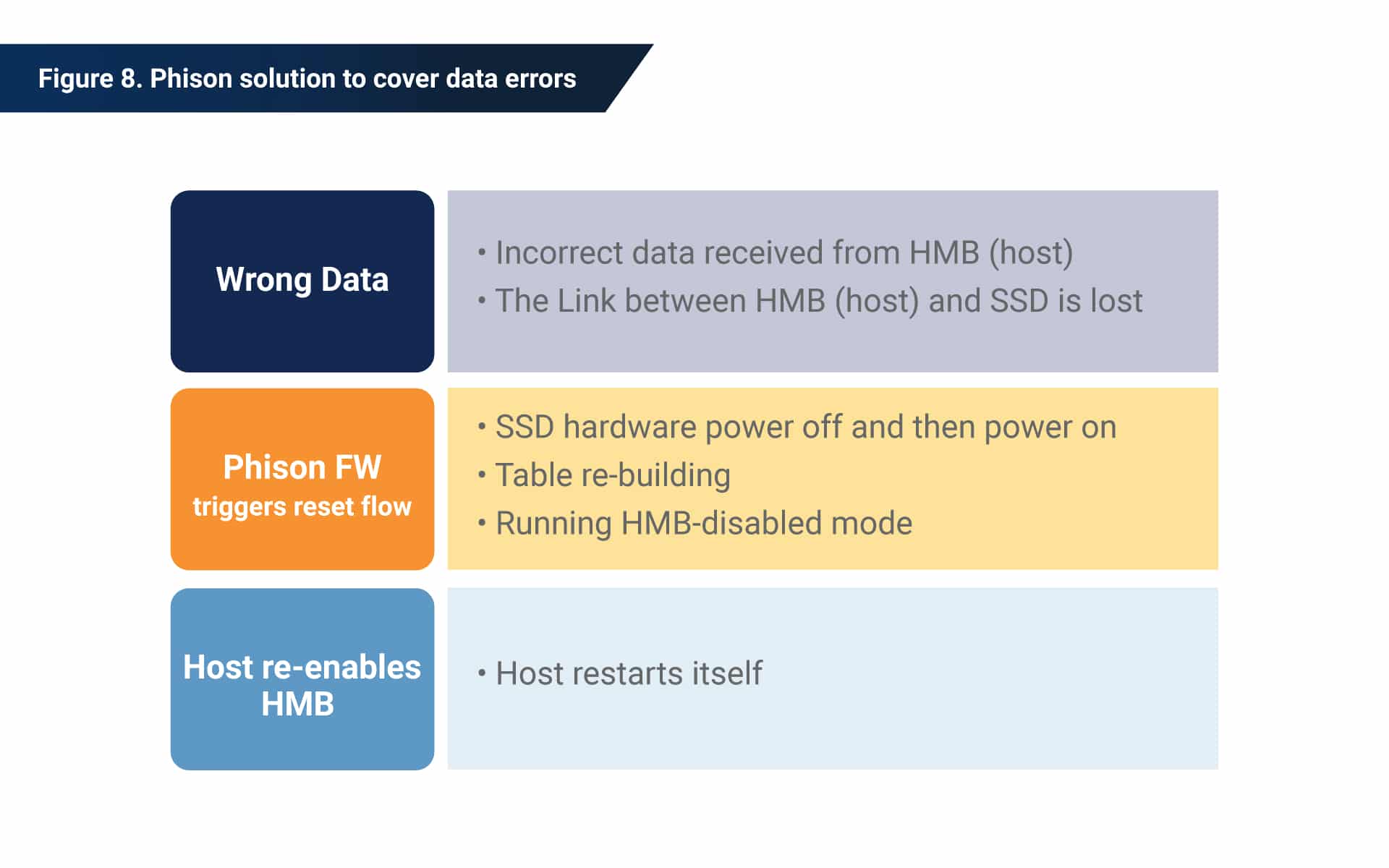
As defined in the NVMe protocol, flash controllers must guarantee zero chance of data loss or corruption if the SSD is removed unexpectedly when using HMB. To fulfill this standard, Phison’s controller solutions use proprietary firmware designed to eradicate data transmission errors and confirm data integrity during operations.
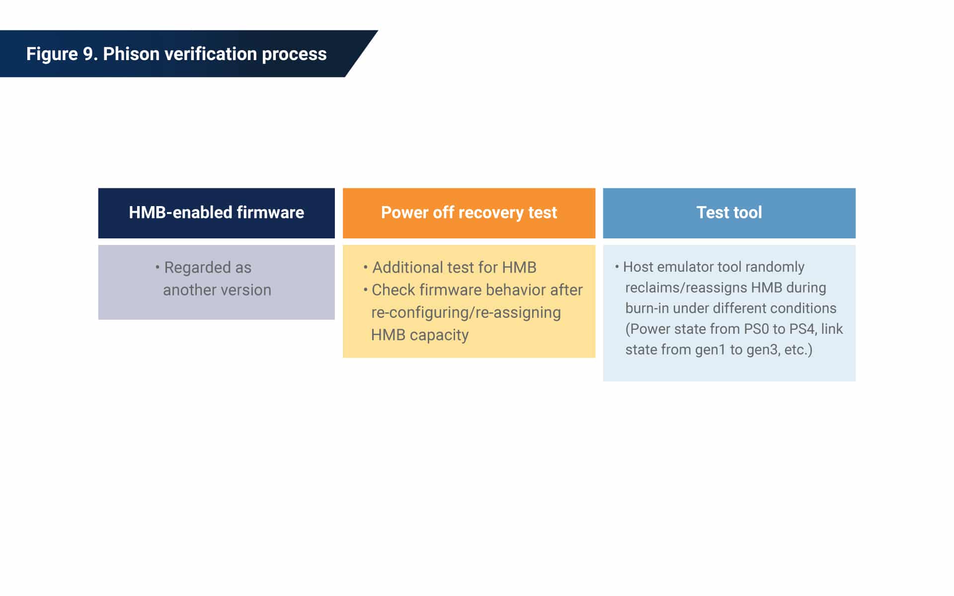
In addition, Phison draws on its vast knowledge and experience to test and validate its SSD designs. Phison conducts both controller-level and system-level tests for thorough functional and physical verification.
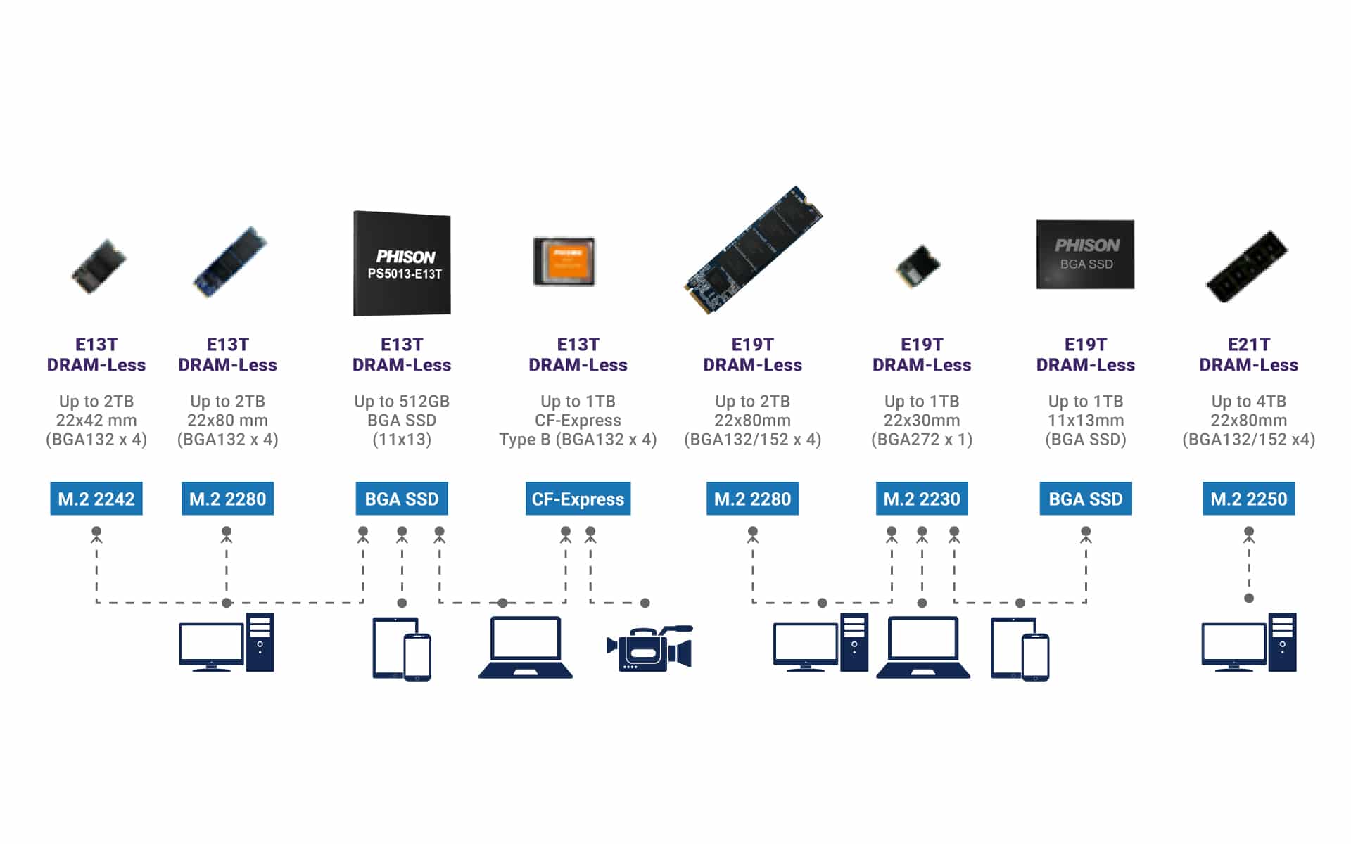
Below, the chart shows what DRAM-less products Phison makes that fit into variety of industry applications. Find out more at phison.com.