This article is the third and final in a series that takes an in-depth look into one of Phison’s most critical offerings: the integrated circuit (IC). Our second installment introduced basic IC design processes with an illustration of a NAND Flash controller IC functional block diagram. In this last piece, we will take you one step further into the Phison world of IC design.
As we discussed in our previous article about IC design, it is important that ICs are designed “around” target applications. To do that, designers must understand the functions that the circuits need to achieve. Only then can they put together a list of detailed specifications to closely address quantitative and qualitative variables like power parameters, memory capacity, thresholds, environmental adaptability and so on.
Specific function blocks and requirements can vary greatly depending on the intended use case and application. However, some general function blocks can be common in the design for specific applications. To illustrate this, let’s take a look at some examples of IC design for AI and 5G applications before we move on to flash memory controllers.

IC design for AI and 5G applications
For many AI application-centric ICs, a critical function block is the digital signal processing (DSP) engine. This is a hardware engine responsible for performing complex mathematical operations required for algorithms such as matrix multiplication and convolution, which are essential steps of computation that happen all the time and in large volumes during computer machine learning and deep learning.
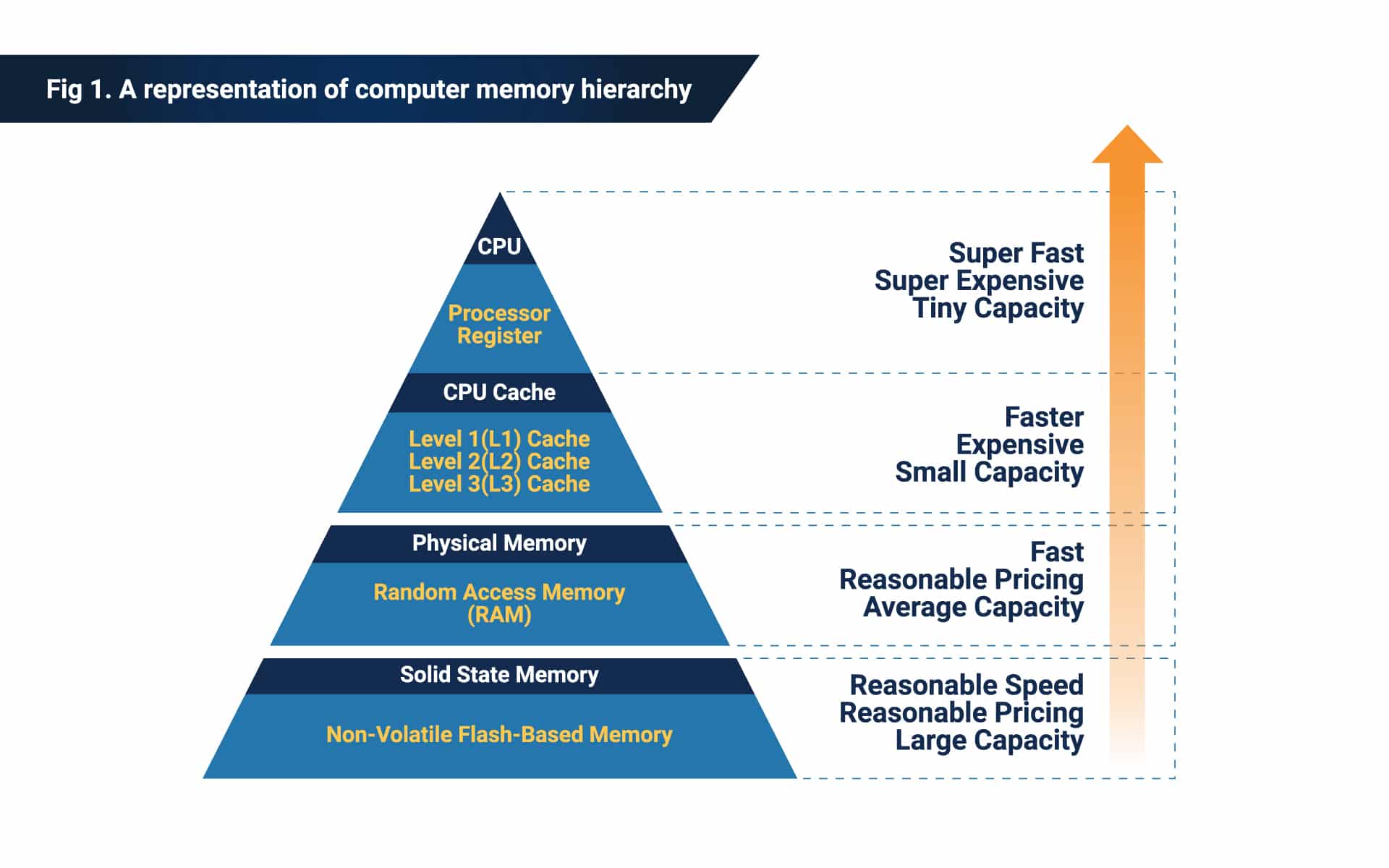
On the flip side of the computing-end in a computing system is the memory-end. Every computing system needs some sort of hardware space to temporarily store the intermediate parameters or calculation results. For AI applications, it is crucial that the temporary data generated between calculation and training can be quickly retrieved or put aside for later use. Therefore, most IC chips designed for AI applications require top-tier memory hardware and a good memory interface that makes fast-paced decisions while equipped with lots of registers that can store single bits of data at extreme speed.
On top of speed needed for processing and data storage, some extra speed can be valuable as AI application-centric ICs are often equipped with so-called “hardware accelerators” to support highly demanding workloads like neural network inferences. These accelerators are usually specialized circuits appended to the main processors, which are often busy and burning from bigger tasks, to execute specific calculation missions in parallel. This offloading effect from the accelerators helps improve the overall performance of AI applications by increasing the efficiency of the chip while reducing the energy consumption and latency caused by switching between tasks within the main processor.
As another example, let’s consider 5G application-centric ICs. The focus of this type of IC is mostly to enable high-speed wireless connectivity and data transfer. Key function blocks in the design can include a digital baseband processing unit, which is responsible for encoding and decoding the wireless signals, and a radiofrequency (RF) front-end, which takes care of the antenna and analog signal transceiving required during wireless communication.
In addition, ICs designed for 5G often support advanced features such as beamforming that directs wireless signals to specific devices via the control of multiple antennas. To implement such control mechanisms, a MIMO (multiple-input, multiple-output) function block must be implemented within the circuitry to properly direct the signal sequence from multiple antennas.
Despite the difference in targeted applications, certain aspects and processes used to design an IC create correlations between seemingly disparate IC types. For instance, both AI ICs and flash memory controller ICs require efficient memory interfaces to achieve optimal performances. The distinction is merely where the affiliated memory devices fall on the memory hierarchy. In terms of 5G ICs, the design of a robust MIMO signal system shares subtle similarities with the implementation of a first-in, first-out (FIFO) buffer to control data flow in a NAND flash storage front-end. While there is no direct connection between the two designs, they do both involve distinct buffer circuits that generate desired output with manipulated inputs.
IC design for flash memory controllers in SSDs
A generic SSD NAND flash memory controller IC includes specific function blocks such as:
-
-
- Front-end interconnects
- A central engine
- A buffer and storage media management unit
- Peripheral interconnects
- Multiple encryption engines for reliability assurance and security features
-
These blocks work together to ensure the efficient operation of the SSD as a reliable data storage device. To better illustrate how that happens, we’ll use an analogy of a train station. Just like the way a train station has different areas or sections within it for travelers, the operation of an SSD to service data can also be divided into several parts: the front-end, middle-end and back-end.
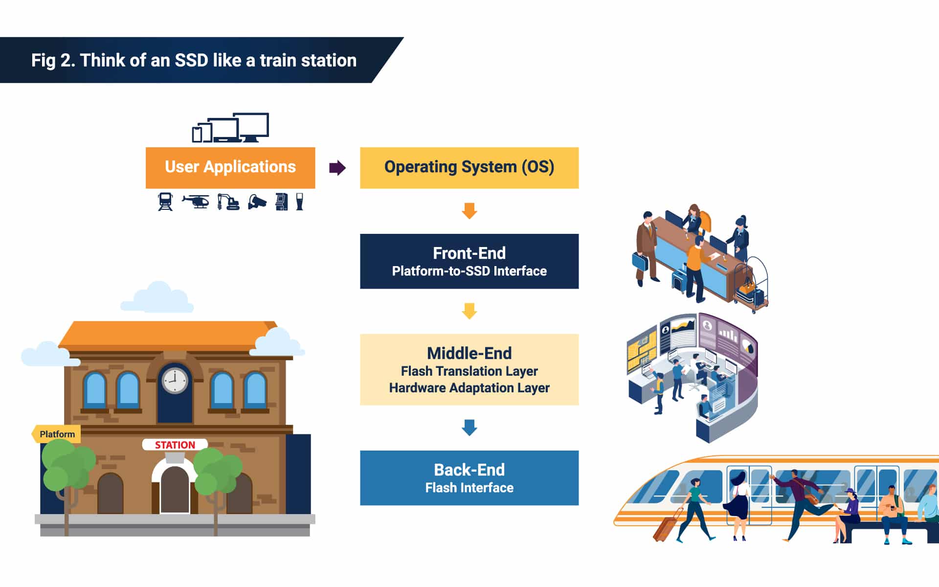
The front-end
Think of the front-end of an SSD like the front lobby of a train station. Similar to a station lobby, where services include ticketing, baggage storage or even janitorial services, the front-end of an SSD serves as data’s entry point with many preliminary processing services for incoming signals. These services include establishment of a signal link through a targeted transmission interface (which may be SATA, SAS or PCIe), protocol-abiding digital signal translation and assorted routines of connection verifications.
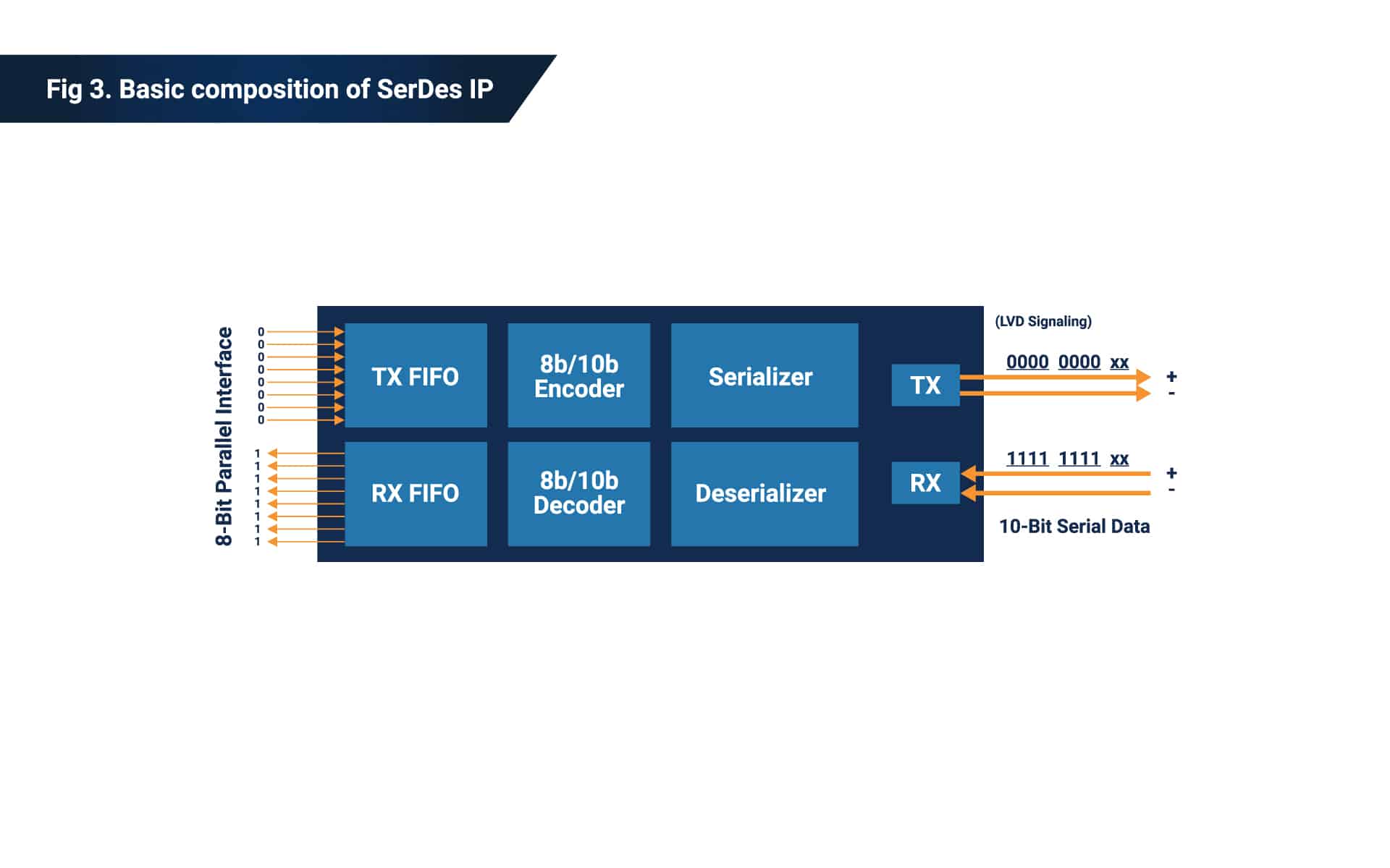
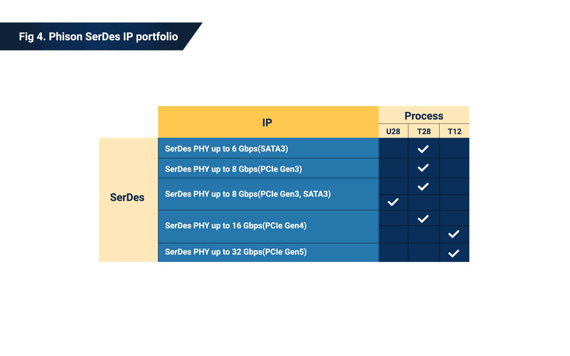
To provide these services, many generic and patented miniature circuits, often abbreviated as IPs, must be packed onto a NAND flash memory controller IC chip. One example of a front-end IP on Phison’s own SSD controller solutions is the SerDes (short for Serial-and-Deserializer) that is responsible for converting incoming parallel data bits—meaning they come through different physical pins at the same time—into a serial bitstream and vice versa. The composition of a SerDes includes a FIFO cache for data flow management as well as a pair of coders for protocol conformance. Phison has its own comprehensive SerDes IP portfolio for mainstream SSD transmission interfaces built on the industry’s best nanometer-scale production processes to fully power its SSD front-ends.
The middle-end
The middle-end is mainly responsible for cache and storage media management. Inside SSDs are two key memory components: DRAM and NAND flash. DRAM serves as a cache space where temporary data can be placed and NAND flash is the storage media where data is stored for longer periods of time. The middle-end is highly important to an SSD for its function as the center of the system. Just like train station dispatchers or announcers direct passengers to temporary waiting areas or trains for longer journeys, SSD ICs direct data to DRAM for temporary storage or NAND flash for longer storage.
To do its job as the central dispatch office, a Flash Translation Layer (FTL) and hardware adaptation layer must be implemented to collaborate on data placement on the memory devices. The FTL is responsible for mapping data on its account book to the correct physical location on flash memory. Likewise, a similar mechanism of table management and mapping is also adopted for temporary data to DRAM. Both FTL and hardware adaptation layers are critical firmware features that can seriously affect the overall performance of an SSD. They’re driven by a powerful central hardware engine that must be delicately planned within the design of a controller IC.
To tackle the needs in the middle-end, Phison has many hardware IPs that provide unique ways of assisting the central dispatcher. They include the CoXProcessor™ and Memory Interface IPs that allow Phison’s NAND flash controller ICs to outperform others with products in each generation.

The back-end
The back-end of a NAND flash memory controller IC is all about the NAND flash memory. As mentioned earlier, the NAND flash memory chips are the trains in our train station analogy. In-train services are just as important in terms of the overall traveling experience as the help and directions given in stations. A big part of NAND flash controller IC design is focused on these in-train services, which include NAND interface protocol conforming, endurance sustaining and error correcting.
The ability of a NAND flash controller to conform to NAND flash interface protocols is like having an adept train driver who can operate different train models flawlessly and efficiently. Phison has a strong IP portfolio compatible with the newest interface specifications from mainstream protocols ONFI and Toggle. With the accumulated hardware and firmware IPs, Phison’s NAND flash memory controller ICs drive NAND flash with an effortlessly smooth pace and control.
Just as we’ve all experienced during our travels, sometimes we make mistakes finding our seats or even boarding the right train—and so does data in the form of electrons within NAND flash memory. Electrons can occasionally escape from NAND flash cells due to their inherent physical characteristics, and that can lead to data bit errors during operation and over time. Therefore, maintaining high endurance and reliability of NAND flash is another crucial requirement for a good NAND flash memory controller IC back-end design.
Choose Phison ICs for high reliability and quality
Phison selects the most premium NAND flash solutions from the market to guarantee the best innate lifespan of its high-end SSD products—and the company has reinforced its legacy of quality with a strong portfolio of advanced Error Correcting Code (ECC). Much like a professional and helpful on-train service attendant assists passengers, Phison’s advanced ECC handles those escaped electrons and NAND flash bit errors with ease based on generations of constantly improving firmware algorithms and hardware engines for dedicated mathematical computations.