This article is the second in a series that will take an in-depth look into one of Phison’s most critical offerings: the integrated circuit (IC). Our first installment explored what ICs are and how they’re classified. Now we’ll delve into how ICs are designed.
The integrated circuit was first developed in 1960, and contained just five resistors and four transistors (mini-switches or valves that become conductive when connected to electrical voltage or current). Seems simple, right?
Things changed quickly, however, with the number of transistors and other components on the IC growing rapidly—so rapidly, in fact, that in 1965 a wise man named Gordon Moore made a now-famous observation. He predicted that the number of transistors in an average IC would double every two years. He saw how in just a few short years the semiconductor industry was skyrocketing, and how the size of transistors kept shrinking as manufacturing processes and technological knowledge advanced.
“Moore’s law” was pretty accurate for more than 40 years. In the early 2000s, the estimate began to slow down because the technology of silicon transistors was pushing the physical limit. Transistors are about as small as they can physically be today, and have grown ever-more-complex with 3D architecture and other technologies.
That doesn’t mean computer chips have stopped evolving, however. The technologies that enable semiconductors and IC components are still advancing exponentially. A digital IC today can easily contain more than 100 billion transistors per chip. ICs built with this many transistors are complex beyond belief. It’s difficult to even imagine a pipe system, like we did in our previous article, with a measly 1 billion valves, let alone 100 billion.
Instead of trying to visualize the staggering complexity of a modern IC, we’ll take a look at how these chips are designed, step by step. There are five main phases of IC design:
-
-
- IC specification and functional design
- RTL coding
- Gate-level netlisting
- Layout production
- Taping out
-
While the terms might seem daunting at first, they can all be explained with a simple analogy: the designing of a house (Figure 1).
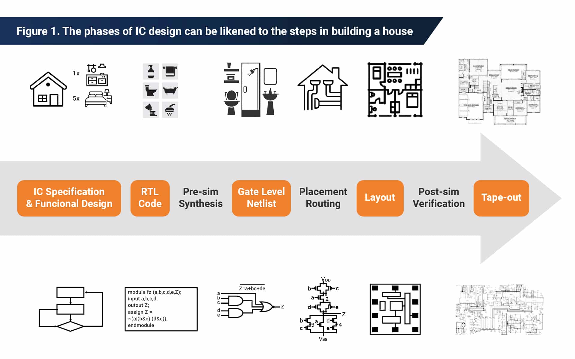
Fig 1. The phases of IC design can be likened to the steps in building a house.
Phase 1: IC specification and functional design
When designing a house, it’s important that the homeowner and architect communicate up front about all the functions and features the owner wants the home to have. It’s all about planning the project—and it works the same way in IC design. The IC designer and the stakeholders need to discuss the desired specifications that will enable the features and capabilities needed by the target application. For instance, in a typical NAND flash controller IC, the major function blocks include front-end interconnect, central engine, buffer and storage media management, peripheral interconnects, and security features (Figure 2).
While a functional block diagram as shown in Figure 2 may seem straightforward, there are in fact an abundance of detailed conditions and parameters that need to be established up front and reviewed carefully before hardware designers can proceed with the next phase.
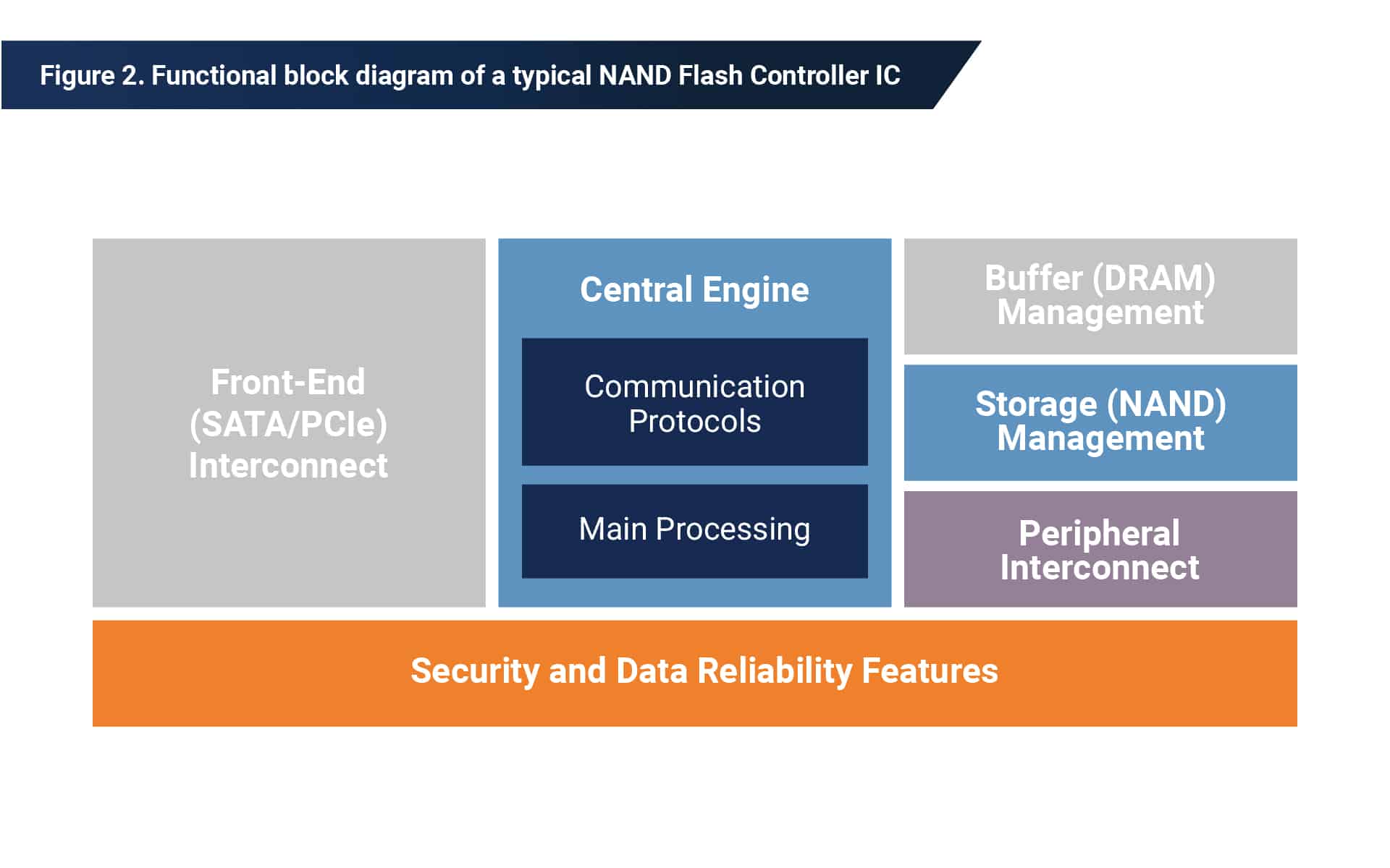
Fig 2. Functional block diagram of a typical NAND Flash Controller IC.
Phase 2: RTL coding
While the first phase was all about planning, this phase and the next are considered the execution parts of the IC design process. With a functional block diagram in hand, designers create drafts of register-transfer-level (RTL) code that can theoretically carry out the specifications the team agreed on during phase 1. The RTL code is a high-level representation of the IC, and is used to “describe” the entire system in its simplest form in these early stages.
RTL code is a low-level coding language that allows designers to essentially present different ways of putting together the IC “puzzle.” To continue the house-building analogy, the RTL coding drafts are basically lists of combinations of design components, much as a house plan would specify flooring and cabinet style and materials, ceiling or wall trim and plumbing fixtures. By evaluating the RTL code drafts, the design team should be able to deduce the theoretically optimal composition of each block in the system.
Phase 3: Gate-level netlisting
Once committed to an RTL code draft, the design team is now ready to conduct a gate-level netlist of the RTL code result. This means that the designers map out the RTL code result with logical gates. This map contains all the delays and logics that will be in the final system. It’s similar to a 3D simulation of a house with all the design elements and fixtures installed so the team can see how it all works together.
While 3D graphic simulations allow home designers and stakeholders to visualize the design, gate-level netlisting helps to clarify all the logical configurations in accordance with the RTL code plan. With the final version of the netlist in place, designers should now have a high confidence level in the overall design feasibility, as most of the tricky design decisions would have been discussed and resolved in this phase. A gate-level netlist allows you to test the final design via simulation.
Phase 4: Layout production
Once the gate-level netlist is finalized, hardware engineers can now simulate the placement of circuits, transistors and other components to produce a detailed layout of the IC. This work of connecting all the necessary function blocks and their respective components is analogous to the linking and routing of a home’s plumbing and lighting systems. By the end of this phase, the IC design team has a detailed “master blueprint” and the actual construction is almost a go.
Phase 5: Tape-out
Tape-out is the final phase of the IC design process—the last stop before the IC is sent out for manufacturing. This phase involves creating a photomask of the circuit. A photomask starts with a solid plate, typically made of quartz or glass. Taping out is the process of coating that plate with an opaque film that has cut-out spaces or holes where light can shine through (Figure 3). IC fabricators use photomasks to produce patterns on a silicon chip. You can consider it the “master template” of an IC design.

Fig 3. A prepared IC photomask.
At this point, the home-building analogy begins to break down a bit. The construction of a house according to a detailed blueprint can still face many challenges and unforeseen issues. In IC design, there’s less uncertainty because simulations created with electronic design automation (EDA) software can mimic the realistic operation and functionality of the system design. While anomalies can still occur, most potential issues can be anticipated and resolved before actual production, saving a lot of time, effort and money.

Phison is an industry leader in customized IC design
Phison’s NAND flash storage solutions and proprietary IC design have evolved to meet the changing needs of modern enterprises and fluctuating market demands. With its proven design prowess and rich experience in innovation, the company is ready to help revolutionize next-generation applications across the world.
Stay tuned for our third and final installment of the IC 101 blog series, where we’ll explore the approach Phison takes in IC development.