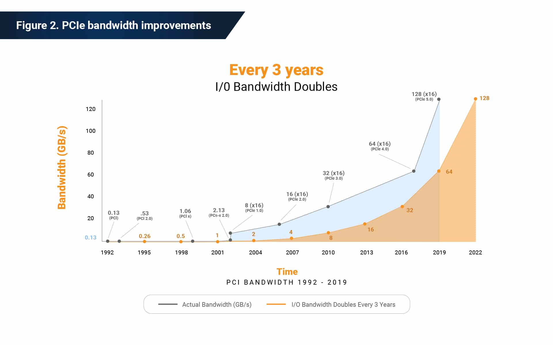
It’s not news that PCIe has been the standard interface for connecting high-speed peripheral hardware components on computer motherboards for the past decade. While the standard has been going through a steady transfer rate upgrade and generational changes every 3 to 4 years since the earliest release, the PCIe 4.0 arrived in 2017, attracting waves of attention and enthusiasm for technological innovation. From a data storage standpoint, the “Gen 4” interface unleashed the long-standing bandwidth ceiling of approximately 3 GB/s of NVMe Solid State Drives (SSD) built upon the PCIe 3.0 standard. The interface upgrade encouraged many vendors to push for better design to accommodate the Gen 4 interface and address the bottleneck between processor-tier and storage-tier hardware solutions.

The PCIe interface and Gen 4 basics
From the peripheral component perspective, the PCIe interface is what we see as the “front-end” within the component module development process. The ultimate goal of a decent “front-end” design is to ensure a robust connection between the hardware module and the computer system through the target interface.
You can separate the design and development process into two phases: hardware and firmware. While it’s easy to question the innovation that goes in the “front-end” design work with PCIe having lasted since the early 2000s, the details within hardware and firmware improvement efforts make mature designs stand out along with releases of each interface specification.
To understand the “front-end” design mainframe, you must first review the PCIe interface hardware configuration basics. For a storage component to connect to the motherboard through PCIe, it adopts one of the hardware connectors usually referred to as x1, x4, x8, and x16 slot configurations. As an example, a Gen 4×4 configuration indicates the connector follows the necessary design and characteristic requirements from PCIe base specification revision 4.0 and at the same time sends data signals through 4 PCIe “lanes.” Each lane is a bi-directional pathway that “flashes” billions of electrical signals within a second. The Gen 4 PCIe lanes perform the signaling at 16 giga-transfers per second (GT/s). While one “bit” of data can be exchanged between a transmission node and a reception node through releases of electrical signals of high/low voltages to represent logical 1s and 0s, 16 GT/s indicates 16 billion times of such execution within one second.

Moreover, PCIe lanes function under the “full-duplex” mechanism. I.e., data transfers in two directions can coincide. Therefore, the transfer rate of 16 GT/s theoretically indicates that a capable PCIe component operating on the fourth-generation connectors can exchange 32 billion data bits within one second within just one of its 32 lanes available for use.
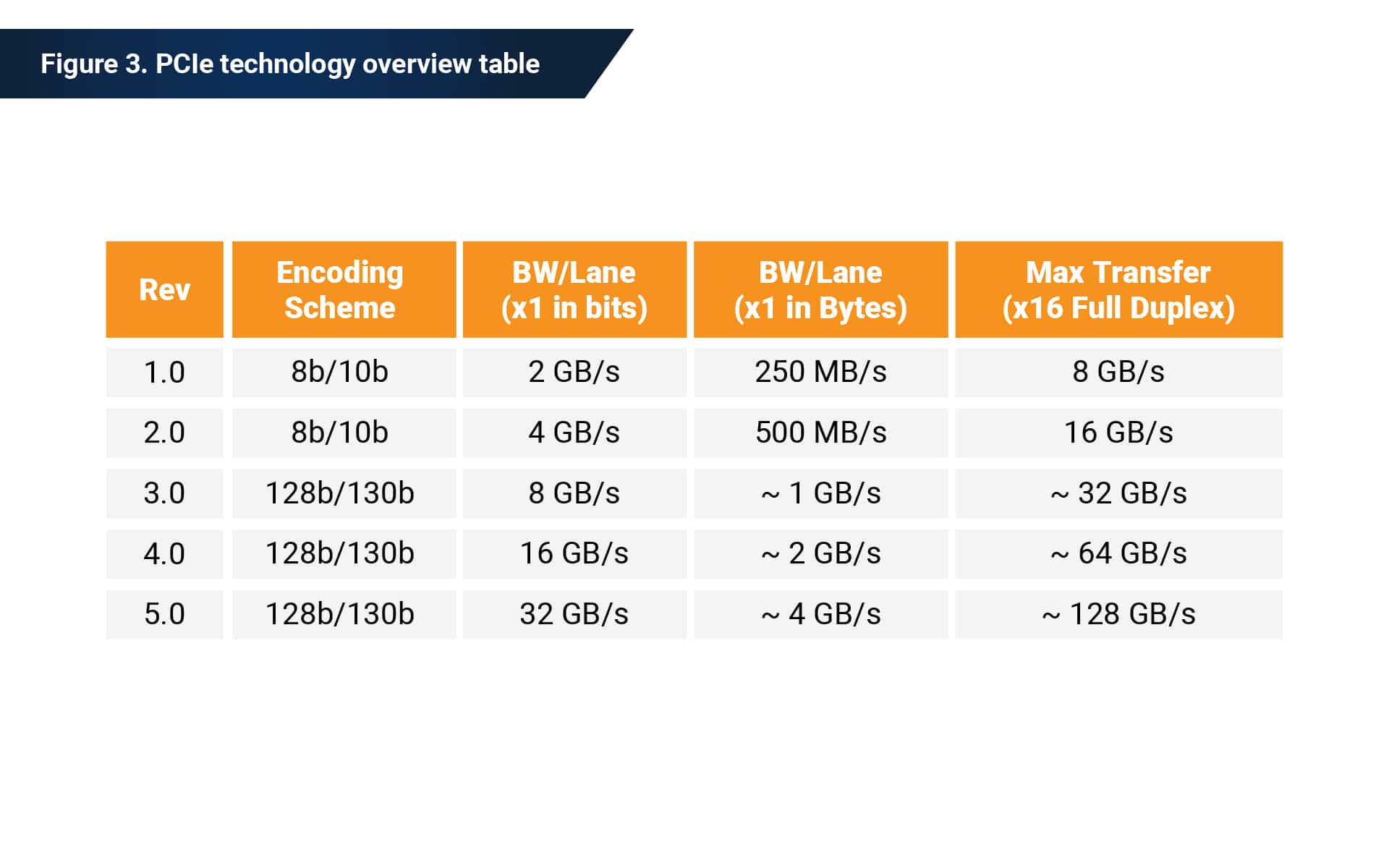
However, the catch to the calculation is that PCIe, like many other data transfer hardware interfaces, protects its data by encoding clock information into the data streams. Starting with PCIe Gen 3, the 128-bit to 130-bit encoding scheme is used for data protection. This scheme requires 2 bits within every 130-bit transfer for stored clock information to help identify and verify the data on the reception side of the link. With simple division and multiplication, 16GT/s turns into a transfer rate of 15.754 billion bits per second, commonly referred to as 15.754 Gb/s of meaningful data bits transfer (neglecting the clock info bits).
Counting in the clock info bits gives the physical bandwidth of 16 Gb/s. It can then be converted at a rate of 8 bits to 1 “byte” into 4 gigabytes per second (GB/s), which is the more commonly used standard data size units in the world of module-level bandwidth and throughout. Furthermore, the total bandwidth under PCIe Gen 4 dictation comes in with scalability up to 64 GB/s, double the maximum throughput from the previous generation of PCIe 3.0.
To put the significance of this advancement in perspective, the data size of a typed character on a computer is 1 byte (or 8 bits), and a PCIe Gen 4×16 interface can exchange a pair of 32-billion-character files within one second. A 1080p HD movie usually stacks up to a file of approximately 10 GB, and 64 GB/s bandwidth allows you to copy three of those from your storage to a computer while moving three out all in one second under ideal data-handling circumstances. Nevertheless, the PCIe flash storage bottleneck remains far below the 16-lane full capability. Mainstream NVMe SSDs in 2021 primarily use the x4 configuration, which puts the physical performance upper bound at 8GB/s.

PCIe specification overview
There is way more to the most widely adopted current storage interface than just performance indicators. The electrical signaling regulated under the PCIe protocol regulates in-depth functions and capabilities, including but not limited to:
-
-
- interface initialization,
- maintenance status tracking,
- interconnect power management,
- lane mapping negotiation,
- interface-level data encoding/decoding,
- and also embedded clock tuning
-
Looking beyond the Physical Layer are two other PCIe specifications that are just as crucial, if not more so, to proper SSD front-end operation; the “Data Link Layer” (or just “Link Layer”) and the “Transaction Layer”. Just as indicated by the word “physical”, many of the capabilities within this layer depend heavily on the hardware design of the storage module. On the other hand, understanding the two layers above helps shed some light on the front-end related firmware modules.

Immediately above the Physical Layer is the Data Link Layer that is responsible to co-work with the Physical Layer to ensure reliable inter-system information exchange. Note the wording of “information” rather than “data” since the engineering emphasis within this layer has shifted from the physical view in data signaling to the logical and more-so firmware view of connection and linking of the physicals. Its collaboration with Physical Layer encompasses power state conveyance to and from Physical Layer, link-level data protection, and error retry/logging services.
The last but not least of the PCIe design layers is the Transaction Layer, which operates on the movement of data packages known as Transaction Layer Packages (TLP). With the generation and reception of TLPs, the Transaction Layer exchanges flow control information with the other side of the PCIe Link. More specifically, it stores link configuration information generated by the system/storage processors and links capabilities generated by Physical Layer hardware. In addition, the handling of TLP is also the primary foundation for both software and hardware-initiated power management mechanism. Understanding the two layers above helps shed some light on the front-end related firmware modules.
All in all, the Transaction Layer bears heavy duties of link processing and power management that call for synchronized hardware and firmware efforts.

The PCIe Gen 4 market overview
With the continuous refinement of the layered design model for the PCIe architecture, the specification has formulated an expandable and scalable data transferring interface that will continue to evolve beyond the current measures. Even with imminent technology advancement toward the next generations of PCIe as Gen 5 storage controller solutions have arrived in the 2021 market (along with emerging Gen 6 discussions), market adoption is what immediately contributes to industry-level storage revenues day in and day out.
Although it’s no secret that the PCI-SIG Workgroup is already looking way beyond Gen 4, the mainstream solid-state storage market is still in the high noon of Gen 4 adoption. Beginning with the consumer market, AMD secured its position as the first system maker to launch its PCIe Gen 4 platform with the X570 chipset at Computex 2019. Within the same year, Phison took the lead in launching the world’s first PCIe Gen 4 flash controller with our E16 solution that put Gen 3 performance out of the rearview mirror, moving data at 5 GB/s throughputs.
On the other hand, Intel announced the arrival of its new platform codenamed Rocket Lake, which may have been later on timing but not in terms of performance for supported PCIe peripherals. From the official benchmark results released by Intel, PCIe Gen 4 SSD combined with the Rocket Lake platform took the Gen 4 performance to the next level in 2020.
Resonating with this breakthrough, Phison launched its refreshed E18 PCIe Gen 4 controller solution later in the same year to boost the Gen 4 record to its peak. It became the world’s first controller solution to clock in at over 7 GB/s throughput. With continued strong partnership with the two world-class CPU/platform vendors, Phison will stay ready to lead the PCIe consumer market and support its partners and customers with cutting-edge storage solutions spanning the desktop, laptop, gaming, and workstation markets.
On the flip-side of the industry, continued growth in both enterprise and data center-grade high-performance computing applications like machine learning, artificial intelligence (AI), and deep learning, has stimulated the server market to reach for more substantial computing power. The need for high-performance storage with dependable consistency and reliability to ensure a stable quality of service is the perfect opportunity for the transition to PCIe Gen 4 storage solutions to be leveraged to fulfill the bandwidth requirements. In addition to the throughput needs, most enterprise and data center grade use cases follow rigid criteria that regulate stable performance with a low tolerance for out-of-spec latency under stress.
To respond to this demand, strong hardware and firmware design prowess to fine-tune for customer applications is required in order for the PCIe Gen 4 transition to happen seamlessly. As a trailblazer in the Gen 4 solution market, Phison’s engineering team has been painstakingly preparing to dive into the cloud and high-performance computing market transition and pursue storage services at the next level by unleashing the front-end bottleneck.
Phison has proven achievements in Gen 4 applications and the quick and timely delivery of Gen 4 SSD solutions for consumer market. We are dedicating same attention and engineering resources to support the Gen 4 and Gen 5 transition in the enterprise market applications.