The role that Solid State Drives (SSDs) play in the storage market is becoming more and more critical. And because of the tremendous advantages SSDs have over traditional Hard Disk Drives (HDDs), SSDs will soon become the mainstream storage solution.
The adoption of SSD is related to the process evolution of NAND flash. Like other semiconductor products, the NAND flash chip unit cost will be significantly reduced by reducing the processing node. Flash memory is also mainly driven by transistor scaling and multi-level cell (MLC) technology. More than one bit can be stored in a single flash cell. Unfortunately, due to the physical characteristics of NAND flash, the reliability will become worse with the scaling down of transistors and the increase of data bits in a single flash cell. Technologies have been developed to cover these side effects.

Read disturb error
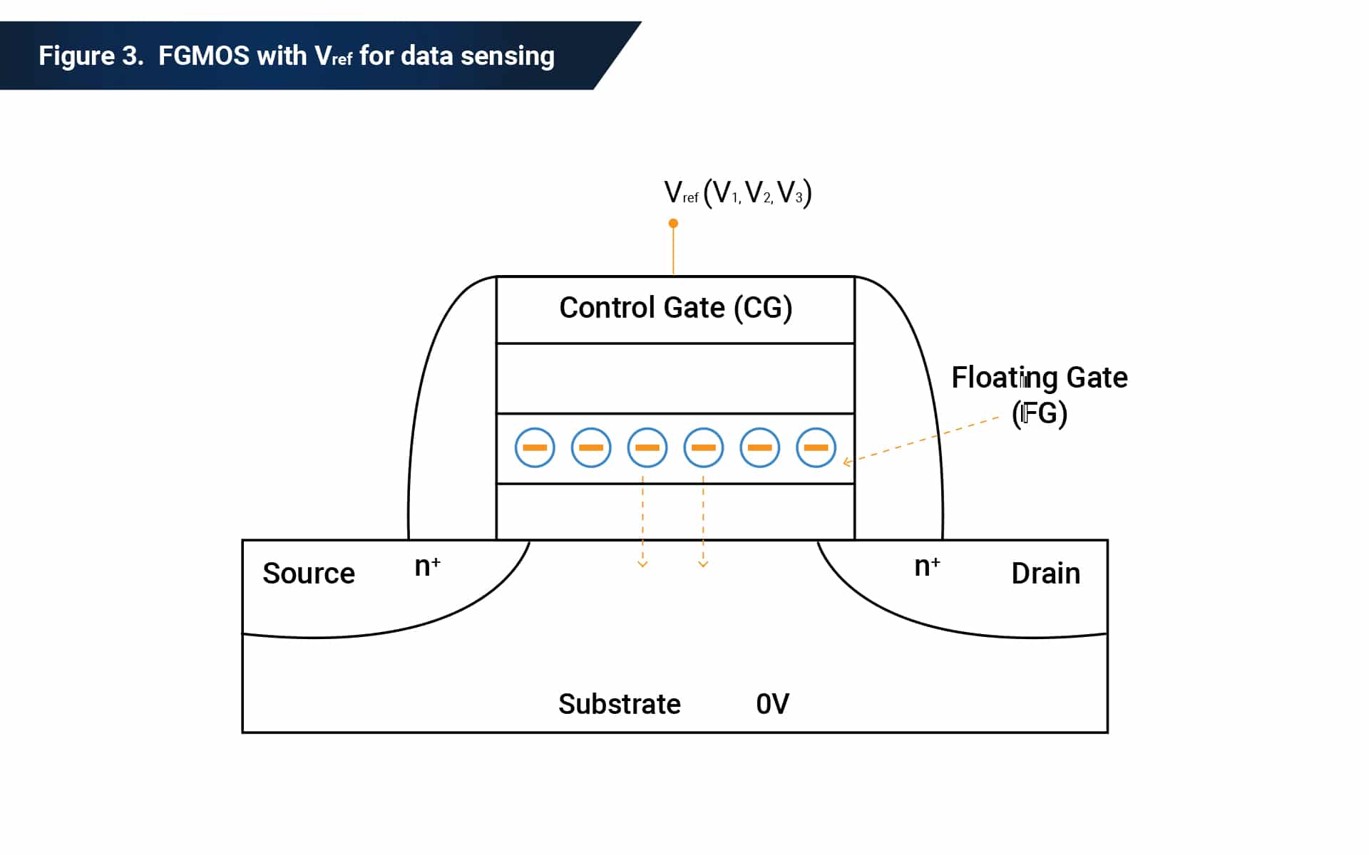
NAND flash memory consists of millions of transistors (MOSFET). Each MOSFET can be regarded as a memory cell. These memory cells store data through a threshold voltage (Vth), the lowest voltage able to “switch on” the memory cell.
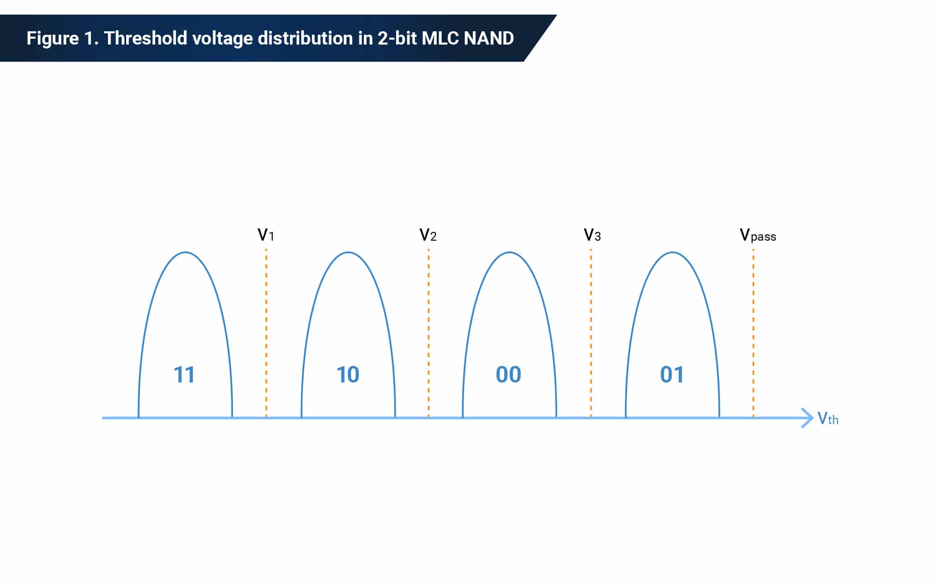
Taking 2-bit MLC NAND as an example, there are four states of data in 2-bit MLC NAND. Three reference voltages (e.g., V1, V2, and V3) that divide the entire range of possible Vth values into these four segments. The region that Vth locates indicates the memory cell’s current state, which is used to identify what data has been stored in the memory cell. An upper boundary of all memory cells’ threshold voltage exists, called a pass-through voltage (Vpass). Vpass is the voltage required to guarantee a memory cell will be switched “on.”
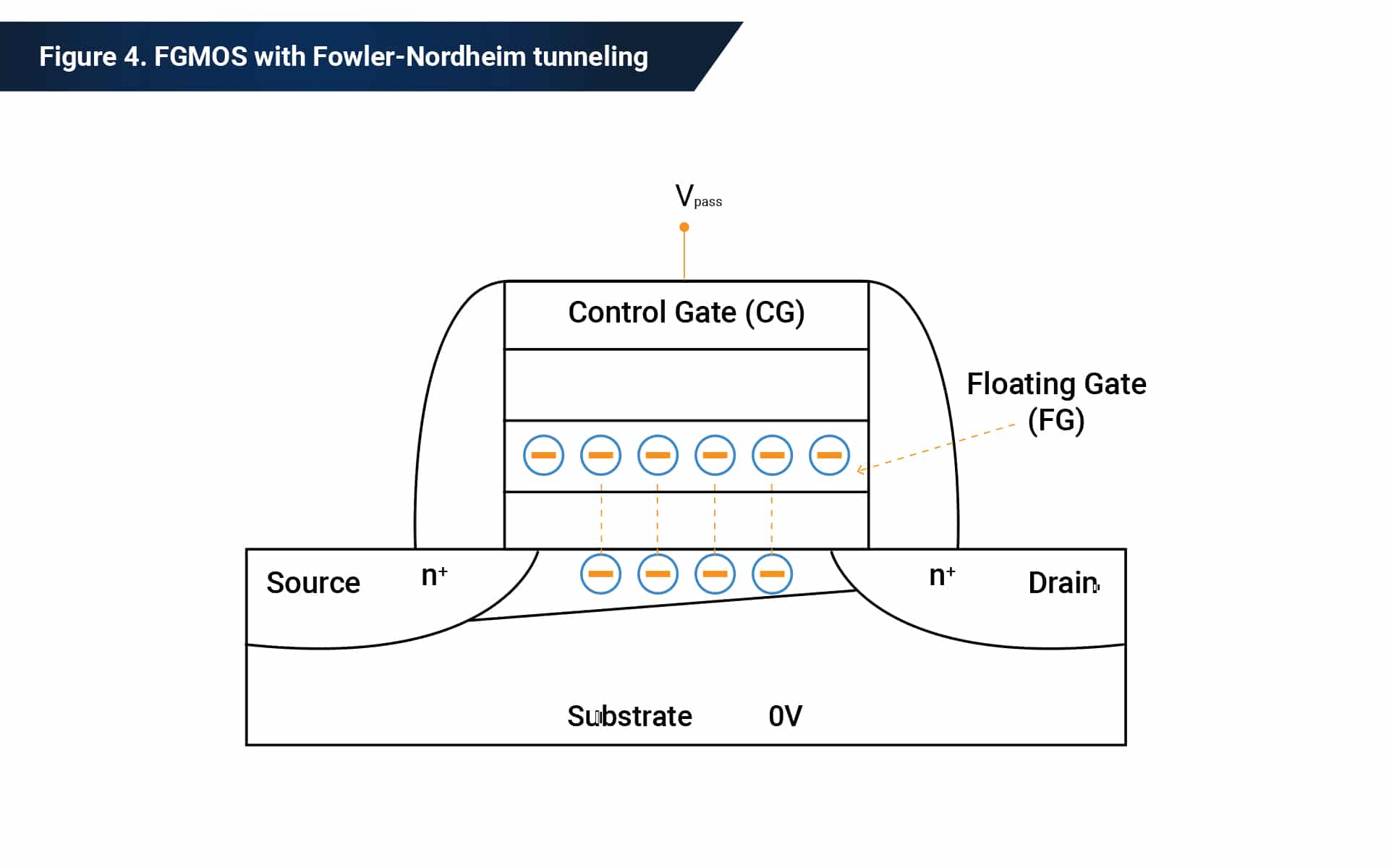
A NAND flash block can be regarded as an array of many transistors. A simple read operation on NAND flash memory is performed by applying a reference voltage (Vref) to the wordline (WL) and then checking the switch ON/OFF status of the selected cell on this WL. Memory cells on the same bitline (BL) are connected with their neighboring cells. Since the cell targeted to be read is just one of them, other unselected cells have to keep their “ON” status to make sure the status of the selected cell can be sensed. Therefore, a pass-through (Vpass) must be applied to other unselected cells on the same BL.
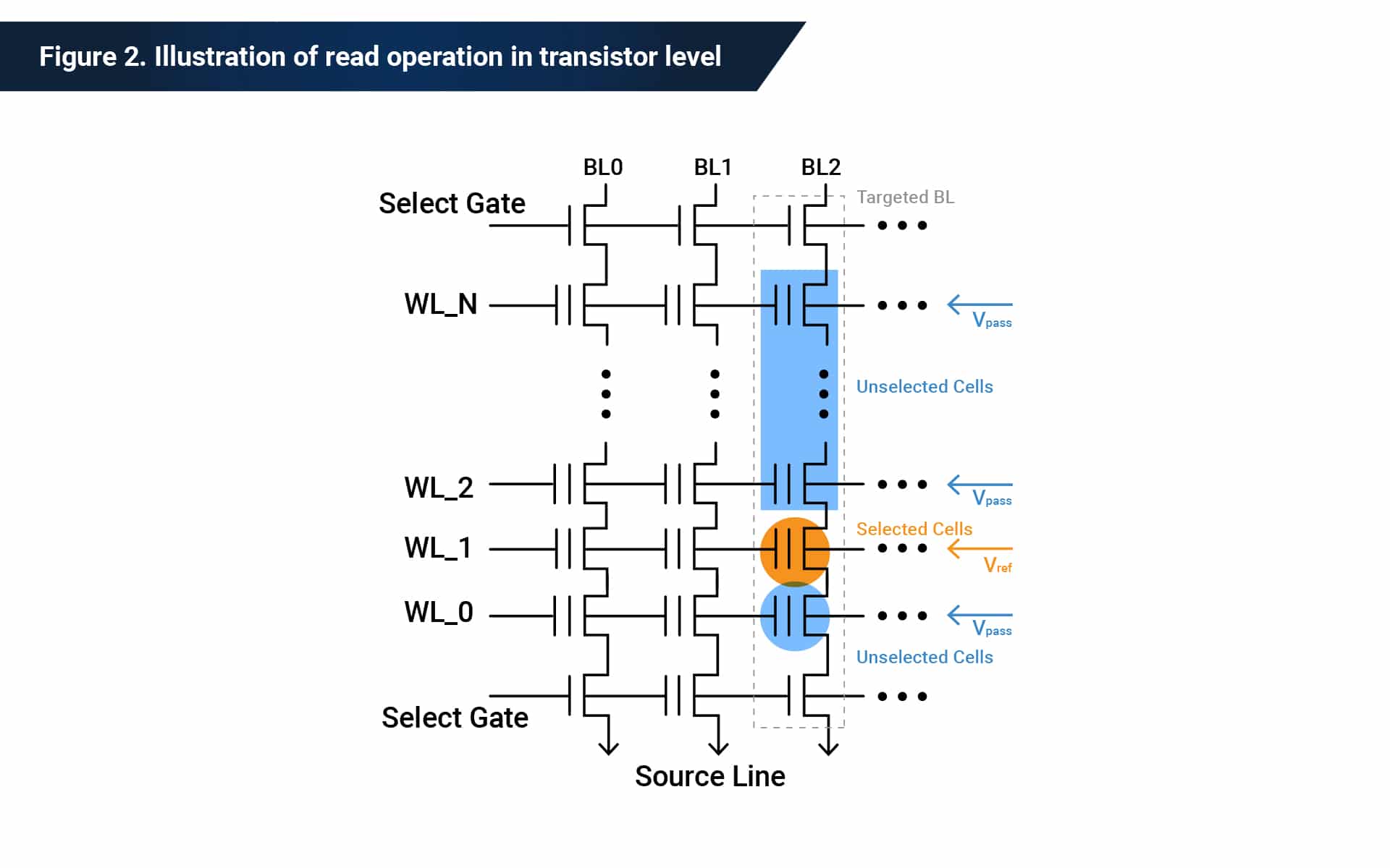
In this way, the threshold voltages of other unselected cells in the same block are shifted to a higher value when a read data operation is performed.
The statuses of unselected memory cells in the same block may be affected because of the Vpass. When a pass-through voltage is applied to the unselected transistors, electrical charges may be injected into the floating gate due to a tunneling effect called a Fowler-Nordheim Tunneling. This effect will cause the shift of threshold voltages of transistors and then result in unacceptable data distortion.
Retention error in NAND flash
Some users write files onto an SSD but do not access them for a long time. Some errors can be detected in these old files. This kind of error is caused by charge leakage over time. This phenomenon is similar to the root cause of a “read disturb”. The charges existing in the transistors determine the threshold voltage level of the memory cell. With the scaling reduction of NAND flash, the size of the threshold voltage window also becomes smaller and smaller. This down-scaling trend raises the probability of threshold voltage level shift due to the retention noise. However, the integrity of rarely accessed data still needs to be guaranteed.
Phison’s SmartRefresh™ technology
To protect the data stored in an SSD, Phison developed a proprietary technology called SmartRefresh™ that uses two primary methodologies:
-
-
- Dynamic Error Bit Monitoring (DEBM)
- Read Retry
-
With the reduction of process scaling, the intrinsic reliability of NAND flash becomes an issue. Error Correction Code (ECC) capability has become one of the most critical topics in the NAND flash industry. Unfortunately, no matter what kind of ECC algorithm is used, there must be a theoretical limitation of its correction capability. If errors can be reduced or avoided before the ECC engine is triggered, the possibility that the ECC engine cannot recover user data is lowered. Dynamic Error Bit Monitoring (DEBM) is a mechanism used for checking the data health status before any data corruption occurs.

Phison’s embedded firmware runs in the background to check the error bit of each block. Once there is a block fail within the criteria set by our firmware (i.e., the number of error bits is over the threshold decided in advance), the firmware performs specific actions on this failed block to guarantee the integrity of user data.
Read retry
Another way to get correct data from a problematic NAND block is to select different voltage levels to perform data interpretation. Fig.1 illustrates a read operation on a 2-bit MLC NAND flash and the threshold voltage (Vth) used to interpret stored data. Phison’s firmware uses proper voltage levels to analyze the data if the current targeted block has been identified as risky. The reliability of the data retrieved by using this methodology depends on the selection of Vth. Phison’s proprietary algorithm determines the best Vth value based on the health evaluation of NAND blocks.
Idle-Time Media Scan (ITMS)
The previously mentioned methodologies can be regarded as a preventive measure and a corrective action, respectively. SmartRefresh™ is a technology that combines these two methodologies to protect user data from unwanted errors due to the physical characteristics of NAND flash. This mechanism is divided into two stages.
Stage one is the Idle-Time Media Scan (ITMS). ITMS is triggered when the Host has entered an IDLE status. Once ITMS is activated, the ITMS is divided into many ITMS cycles, and numbers of sectors are scanned within each ITMS cycle
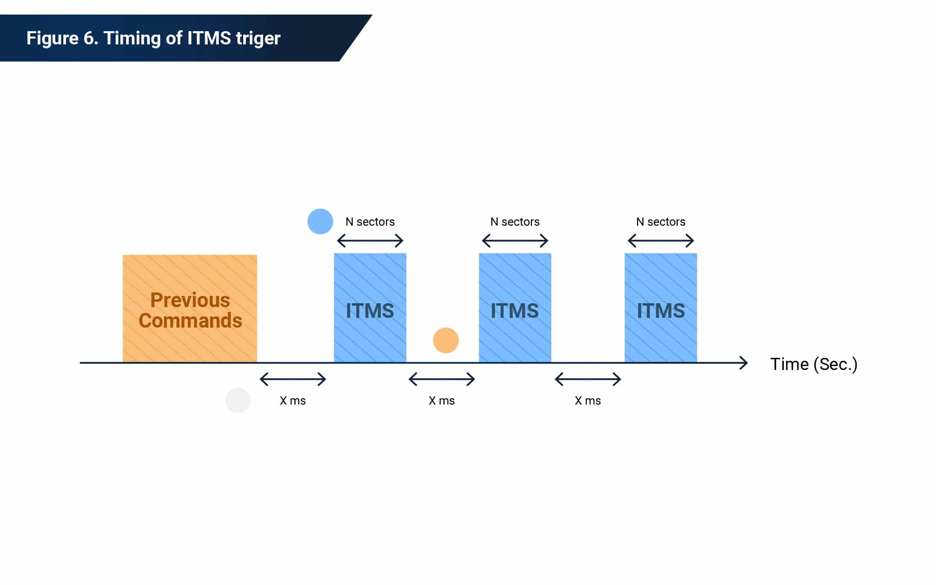
ITMS is a mechanism used to detect if the scanned blocks are healthy after DEBM and Read Retry operations are performed. If any block is identified as an unhealthy block, the valid data inside the unhealthy block is processed appropriately to avoid data loss. Since ITMS utilizes the duration that a Host has entered an IDLE mode to check the health status of stored data, it can be interrupted whenever the Host sends commands to a drive. In this case, ITMS will be stopped, and the next ITMS cycle will launch from an address that has not been checked in the last ITMS cycle.
Run-Time Media Scan (RTMS)
Stage two is the Run-Time Media Scan (RTMS). In contrast to ITMS, the timing to perform RTMS is not limited to IDLE mode. RTMS guarantees that the entire drive is scanned entirely in a specific period (e.g., once every week) even though the Host keeps sending commands to a drive. In other words, RTMS is designed to ensure the data integrity of drives used for processing long-term tasks.
Phison ensures the integrity of your data
Phison’s proprietary technology, SmartRefresh™, offers a reliable mechanism to ensure data integrity, including multiple layers of actions to protect user data stored on an SSD. By adopting Phison’s SmartRefresh™ solution, you can avoid the errors caused by the intrinsic characteristics of NAND flash.