When it comes to electronic devices—and the components that make them up—durability is paramount. Recently, Phison researchers discovered that the industry-standard test methodology used to predict a device’s lifetime was highly inaccurate when testing durability of 3D NAND flash modules. The researchers presented their findings and recommendations to resolve the issue at the 2023 IEEE International Reliability Physics Symposium.
Please note: This article is based on the original paper presented at the symposium. It will be summarized at a high level for less technical readers and then also include some more technical details for readers who prefer them.
A closer look at the original testing method
The longtime industry standard for predicting the lifetime of electronic devices has been a high-temperature-accelerated methodology using the Arrhenius equation. But what does that mean?
“High-temperature-accelerated” means that instead of testing a device’s lifetime by allowing it to age normally, researchers have found a way to accelerate the device’s rate of aging by subjecting it to temperatures that are much higher than its standard operating temperature. That way, they can more rapidly detect failures or defects that might take years to appear under standard operating conditions.
The Arrhenius equation represents the relationship between temperature and reaction rates and how temperature can accelerate those reactions.
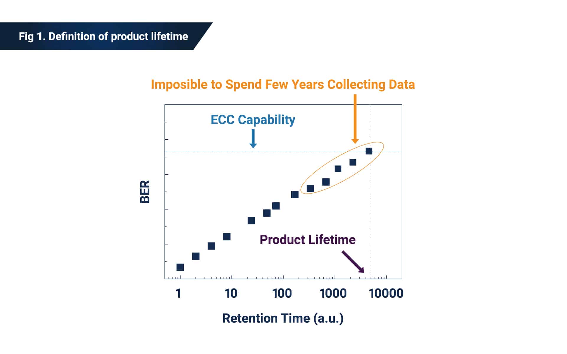
For NAND flash products, lifetime is defined as how long it takes for the device to reach a predefined bit error rate at standard operating temperatures.
For those who prefer a more scientific take, here is a deeper explanation:
The lifetime of a NAND flash product is defined as the retention time at device operation temperature (30oC to 40oC) when the bit error rate (BER) reaches a specific level, which is the upper limit of the error correction code (ECC) capability (see Figure 1).
According to JEDEC documents, the lifetime in electronic devices can be estimated by temperature-accelerated methodology using the Arrhenius equation, which is:
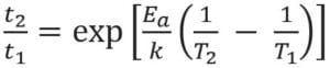
In the equation, T1 and T2 are the bake temperature and device operation temperature, respectively. t1 and t2 are the retention time at T1 and T2, respectively. k is Boltzmann’s constant. Ea is the activation energy and represents the strength of temperature effect on data retention characteristics. Note that larger Ea (larger slope) represents the retention time has stronger temperature effect. In this model, it is assumed that Ea is a constant value and independent of bake temperature. Since Ea is a known factor, which is usually provided by the NAND vendor, the device lifetime t2 at device operation temperature T2 could be calculated accordingly by detecting the memory failure time t1 at bake temperature T1 (see Figure 2).
What Phison found
In their research, Phison engineers discovered that one of the factors in the Arrhenius equation—which had been assumed to be a constant unchanging value—could actually vary in 3D NAND flash devices depending on baking temperature. That’s because the scaling of cell size, the distance between cells and the tunneling layer in 3D NAND flash works differently than those factors in 2D NAND flash. This variance inevitably led to a gross overestimation of the device’s lifetime.
Technical details:
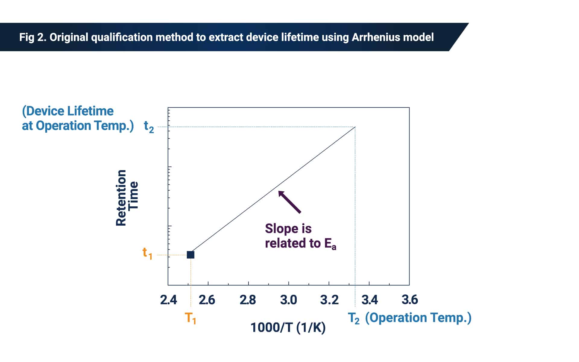
In Phison’s recent study, it was discovered that Ea may not remain unchanged and would vary with baking temperature in 3D NAND flash (see Figure 3).
t is clearly defined as a retention time when the BER arrives at a certain value. In the experiment, various t was recorded in a wide range of baking temperature to extract Ea. The measured t did not follow the conventional Arrhenius model (did not fall into a straight line), and exhibited two-stage behavior. Higher Ea is observed at T > 85oC, while lower Ea is extracted at T < 85oC. Since the evaluated device lifetime through the current qualification method is normally extracted by extrapolating from data points at higher temperature region to operation temperature region, the abnormal two-stage phenomenon would lead to a significant overestimation of retention lifetime.
In general, the value of activation energy Ea is determined by physical mechanism. As a result, the aforementioned two-stage characteristics indicate that the retention failure is caused by more than one physical mechanism.
In Phison’s research, the corresponding physical mechanisms at various retention temperatures and program/erase (P/E) cycle conditions in 3D NAND are validated experimentally for the first time. It has been proven that the peculiar two-stage feature is related to three different physical mechanisms (see Figures 4 and 5).
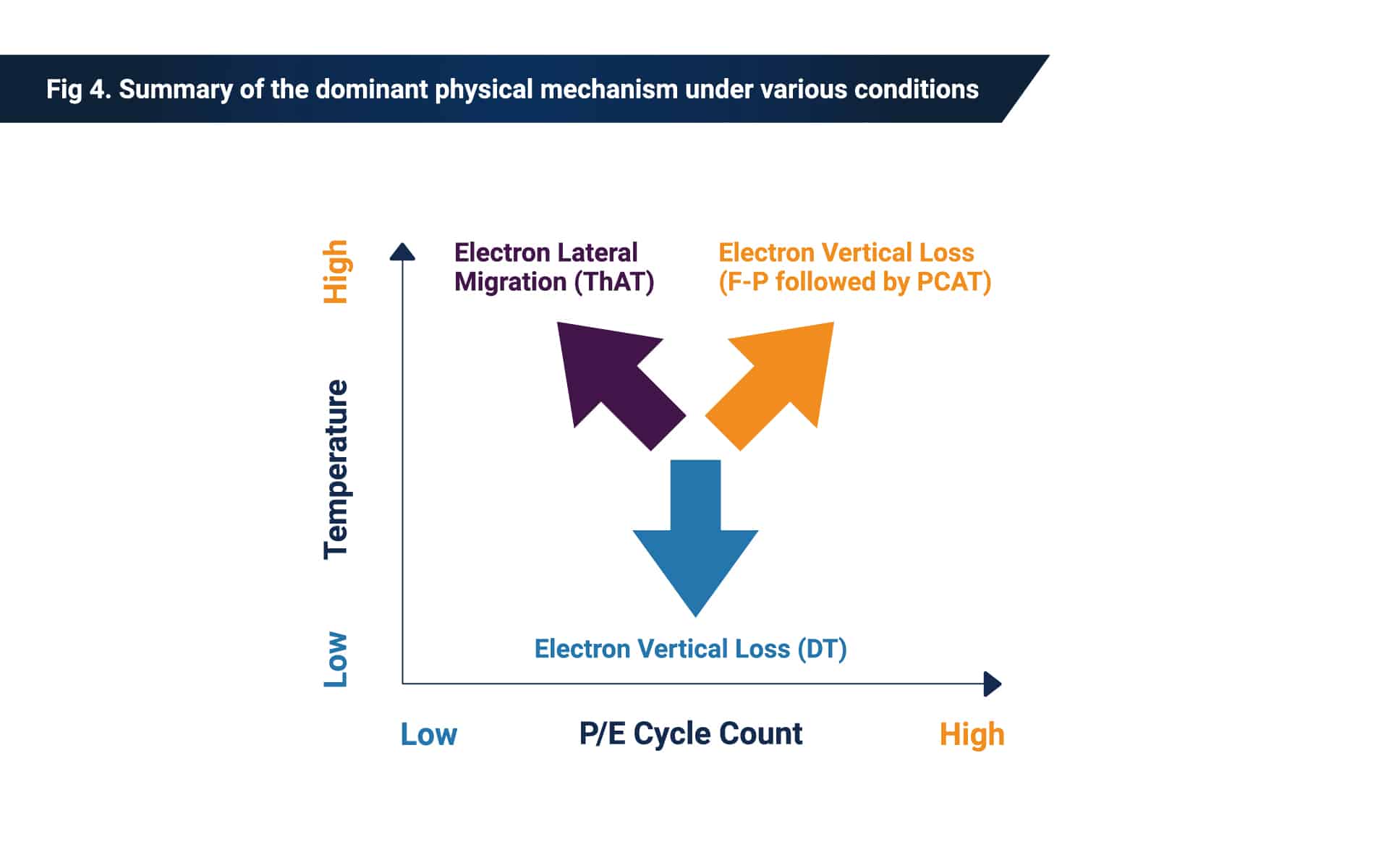
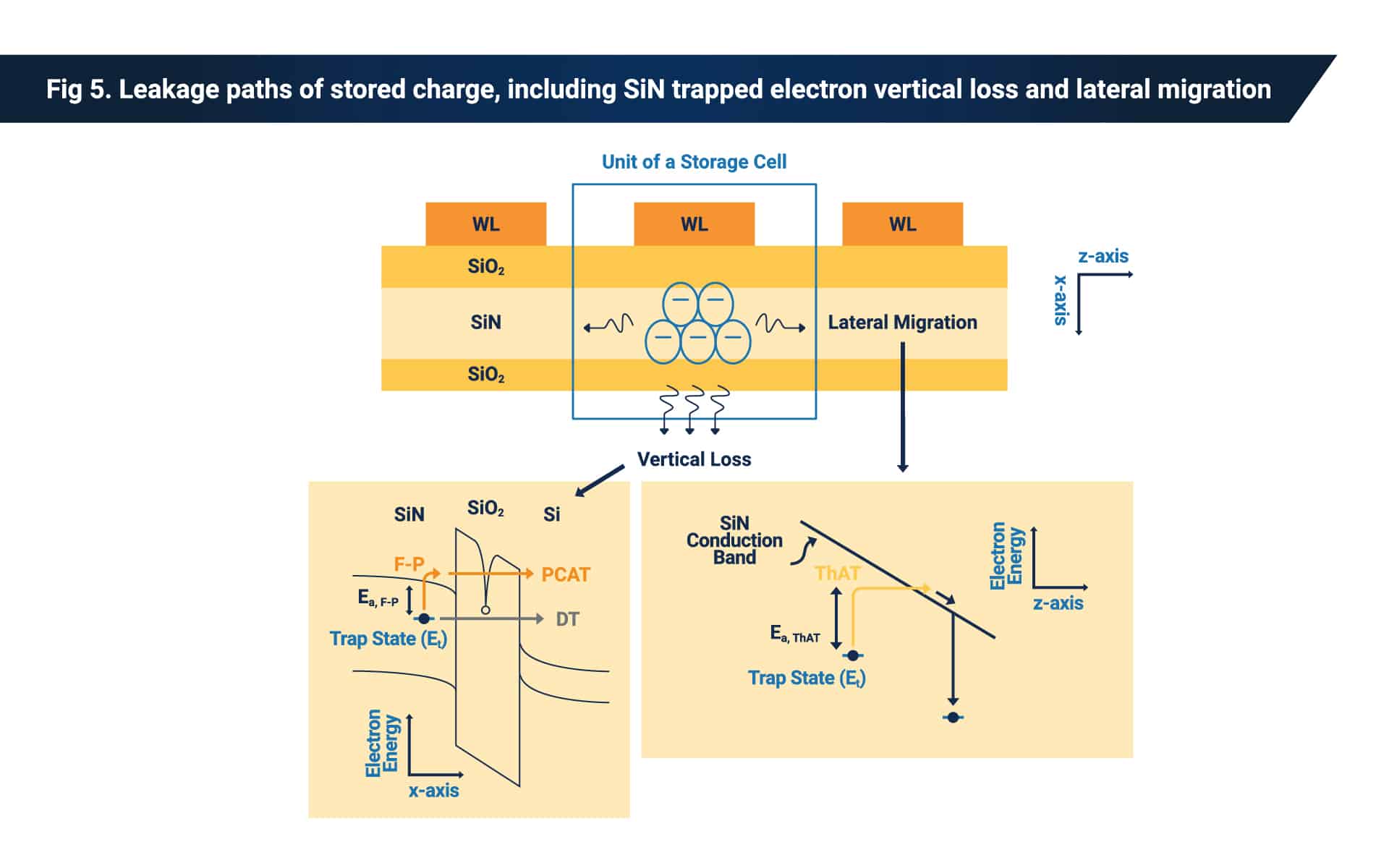
At lower temperatures, the increment of BER tends to be dominated by silicon nitride (SiN)-trapped electron vertical loss through a direct tunneling (DT) process. At higher temperatures, the major physical mechanism depends on the P/E cycle condition. The increment of BER in low P/E-cycled devices is originated from SiN-trapped electron lateral migration via thermally-assisted tunneling (ThAT) while that in high P/E-cycled devices is mainly caused by SiN-trapped electron vertical loss through Frenkel-Poole (F-P) emission, followed by the subsequent positive charge-assisted tunneling (PCAT) process.
Findings lead to new (and more accurate) lifetime qualification methods
Thanks to the Phison team’s research, the inaccuracy of 3D NAND flash lifetime testing was uncovered and explained to the industry at large. In order to resolve the issues of that inaccuracy, the team designed and presented two new testing methods that are now being used in Phison’s reliability qualification process.
Multiple-activation-energies qualification method
This method includes a range of activation energies (that constant that turned out to not be so constant) at different temperatures to get a more accurate lifetime prediction.
Technical details:
In the first step of this testing method, retention characteristics in a wide range of baking temperatures should be implemented to extract multiple Ea values. To simplify for explanation, we assume that only two different activation energies Ea, HT and Ea, LT are obtained (See Figure 6).
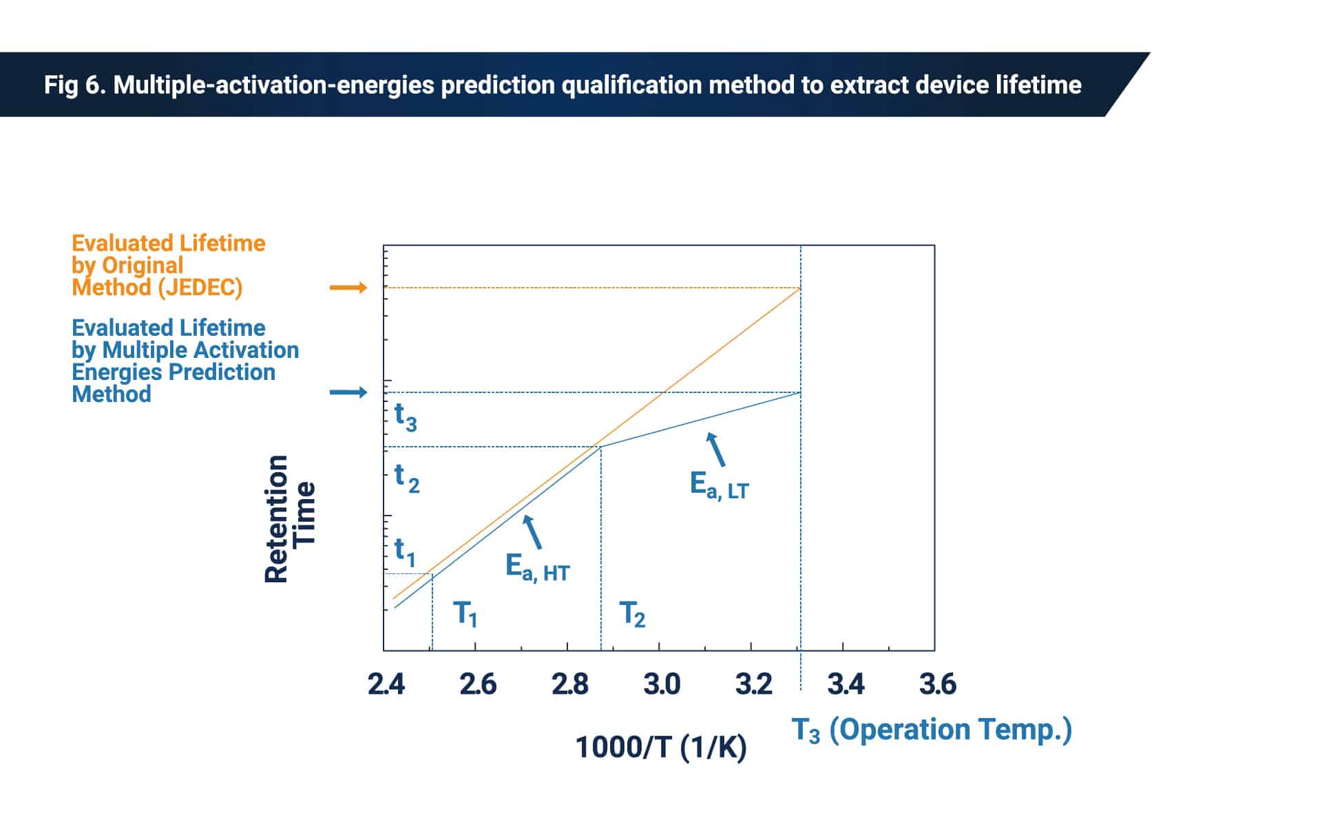
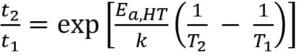
In the next step, device retention time t2 at lower bake temperature T2 could be calculated by measuring the memory failure time t1 at higher bake temperature T1, as shown in this equation:
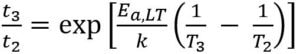
Finally, once t2 is obtained, device lifetime t3 at device operation temperature T3 could be calculated with this equation:
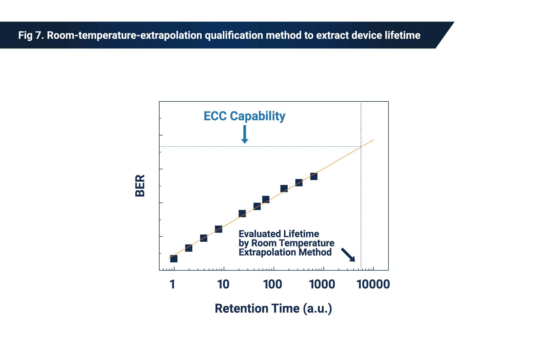
Room-temperature-extrapolation qualification method
This method works by measuring the bit error rate of the device continuously during operation at room temperature. After multiple data points are collected, researchers can predict the device lifetime using a linear extrapolation.
Technical details:
.
Why Phison’s research and recommendations matter
When manufacturers and consumers buy NAND flash or SSDs that contain the NAND flash modules, it’s important to know how long those devices will last. The more accurate and transparent a NAND flash vendor can be about its products, the more its customers can rely on the brand. Thanks to Phison researchers, the lifetime estimates of 3D NAND flash devices and modules will be more accurate—which can help reduce unexpected downtime and other interruptions due to device failure.
Phison is dedicated to continuing research into electronics technology and advanced capabilities to enable and support the applications and use cases of the future.