Historically in the world of mobile devices, the NAND Flash storage subsystem has always been in a tier of its own. This is driven by the requirement for a tiny single-BGA package form-factor and the demand for very low power consumption.
Another reason is the extremely tight level of integration in mobile systems. It requires extensive interoperability and qualification sessions pairing the host platform with each NAND Flash storage device.
The constant push for faster and more capable systems is blurring the lines between the performance requirements of mobile devices and mainstream PCs. This is pushing the need to start exploring other solutions that might enable the next leap forward in mobile devices’ technology.
Before diving into this post, it is interesting to learn some details about The Evolution of Mobile NAND Flash Memory Storage from our previous post. Click the banner below.

Why put PCIe NVMe BGA SSDs on a phone?
The PCIe bus is very versatile and nowadays it is the primary form of interconnection between CPU and expansion boards, networking, storage and peripherals in almost all classes of devices, including mobile.
In mobile applications, PCIe is typically used to connect the CPU with radio modules (WIFI, Bluetooth, cellular modem…). Expanding its use to include storage devices is a logical choice since the PCIe hardware interface is already part of the CPU development, test and qualification program. Also, replicating, validating and testing identical circuits (adding multiple PCIe links) is much more cost effective than investing in design elements that are completely unique (such as the circuitry necessary for UFS).
Adding to the drive for mobile BGA SSD are the recent advances in silicon process nodes and NAND Flash controller architecture. The BGA SSD can now compete from a power/performance (Watts/GBps) standpoint with UFS. Digging deeper still, it becomes evident that we need to question why mobile devices are not using NVMe BGA SSD.
Pace of evolution
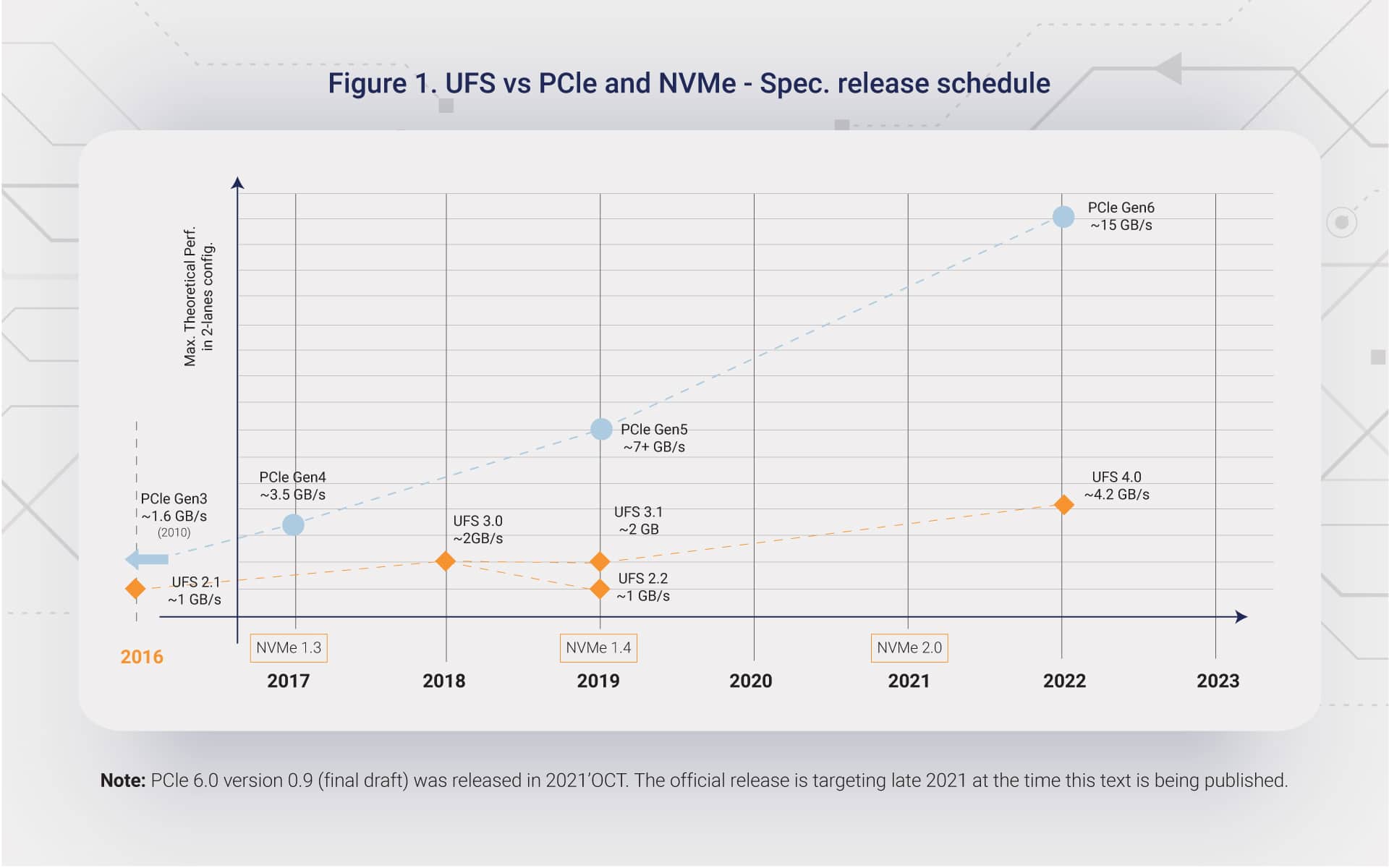
Let’s take a look at the release schedule and data throughput supported by PCIe and UFS over several years of co-existence. The PCIe specifications have been enabling comparable data throughput at least 2 generations earlier than UFS. Our next generation phones could be up to 3.5x faster with BGA NVMe SSD.
Aggressive approach or product maturity?
When a new UFS specification gets published, the whole mobile industry rushes to develop, produce and qualify their products in order to catch the following generation of flagship mobile devices. It usually takes less than a year until the first supplier starts issuing samples of their products.
Considering a similarly aggressive approach to PCIe would result in an immediate and extreme jump in performance within the same time-frame. It could even allow for lane reduction (1-lane) which helps to improve motherboard routing and takes less PCB area, which is critical in such small and dense systems. If that change had happened in 2019, we could’ve had PCIe Gen5 NVMe BGA SSD with 1 or 2 lanes (3.5 or 7GB/s) competing directly with UFS 3.1 (limited to 2GB/s) in 2021.
Though less exciting, but equally important, a BGA SSD improves time to market, because phones benefit from components that have been tested, mass produced and adopted across a wide range of platforms. For example, PCIe Gen3 x2-lanes (1.6GB/s) specification was released 6 years earlier than UFS 2.1 (1GB/s) and Gen4 x2-lanes (3.5 GB/s) was released 1 year earlier than UFS 3.0 (2GB/s).
Development and production scale
A NAND Flash controller IC contains many different functional blocks that are commonly named IP blocks (Intellectual Property blocks) or just IPs.
Two Flash controllers that share the same interface, but are designed for different performance tiers, can share IPs, including the high-speed analog circuitry of the host interface (PCIe, UFS) and NAND Flash I/O.
A BGA SSD benefits from the entire PC and Enterprise ecosystem. For example, an entry-level DRAM-less NVMe M.2 SSD for PCs could simply be repackaged as a BGA SSD. Both SSD would share the same Flash controller, most of their firmware and several other development and test resources. This allows NVMe BGA SSD to benefit from the economy of scale, which enables a better costs for both product lines and much faster time-to-market.
Barrier to entry
Due to the tight level of integration in mobile devices, there is absolutely no room for compatibility problems. Both host CPU and device makers invest considerable effort in making sure all the parts listed on the AVL (Approved Vendor List) have been thoroughly tested and qualified together.
This means that once the industry has settled on interfaces to interconnect components, there needs to be strongly compelling reasons to justify making changes. While PCIe is not the officially adopted standard for the storage subsystems in mobile, it is already being used to connect other subsystems. This greatly simplifies migrating storage to PCIe.
The pioneers and expectations
In our previous article, we mentioned that BlackShark (member of the XiaoMi group) was the first to incorporate an NVM BGA SSD into a flagship phone. Current Phone CPU cannot boot from NVMe, so the Phison NVMe BGA SSD (Phison E13T BGA SSD) was paired with a UFS 3.1 device in a RAID 0 configuration. This allowed the storage subsystem to achieve nearly 3GB/s of bandwidth.
While working with BlackShark, Phison was able to test a wide range of other Phison NVMe SSD to demonstrate the potential for design reuse and even greater bandwidth. Phison expects to launch a Gen4x2 BGA SSD in the 1st half of 2022.
Phison is committed to supporting BGA SSD on mobile phone applications and we are excited about the possibilities the future holds.